Surface treatment for multi-layer wafers formed from layers of materials chosen from among semiconducting materials

Active Publication Date: 2005-06-16
S O I TEC SILICON ON INSULATOR THECHNOLOGIES +1
View PDF3 Cites 194 Cited by
  • Summary
  • Abstract
  • Description
  • Claims
  • Application Information

AI Technical Summary

Benefits of technology

[0025] The present invention provides a treatment process for a multi-layer wafer for which the materials have differential thermal characteristics, the process comprising a high temperature heat treatment step that could generate secondary defects,

Problems solved by technology

However, these known high temperature heat treatments cannot be used on all types of wafers, since there are some limitations associated with them.
The application of this type of high temperature heat treatment to the treatment of single-layer wafers, or multi-layer wafers in which the different layers have differential thermal characteristics, can be problematic.
The very thin layer of SiO2 under these conditions cannot “impose” its mechanical behavior when exposed to high thermal stresses.
“Initial defects” means defects that are already present in materials from which the wafer is composed, or defects generated during one of the steps in initial m

Method used


Image

  • Surface treatment for multi-layer wafers formed from layers of materials chosen from among semiconducting materials
  • Surface treatment for multi-layer wafers formed from layers of materials chosen from among semiconducting materials
  • Surface treatment for multi-layer wafers formed from layers of materials chosen from among semiconducting materials

Examples


Embodiment Construction

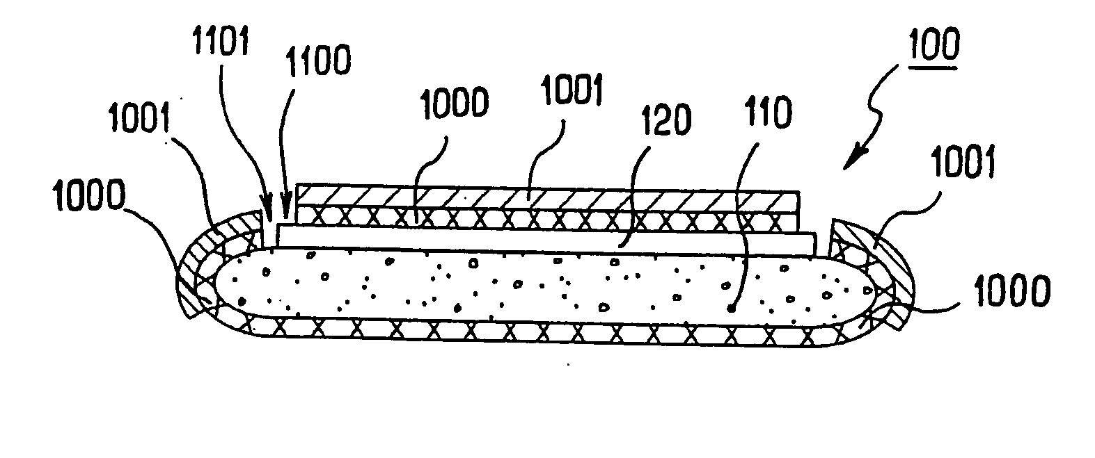
[0040] As mentioned above, the invention is applicable to multi-layer wafers with differential thermal characteristics.

[0041]“Differential thermal characteristics” have been defined above. In particular, they correspond to a difference in the coefficients of thermal expansion of two layers in the wafer, if this difference is large enough to generate secondary defects when the wafer is exposed to a high temperature heat treatment.

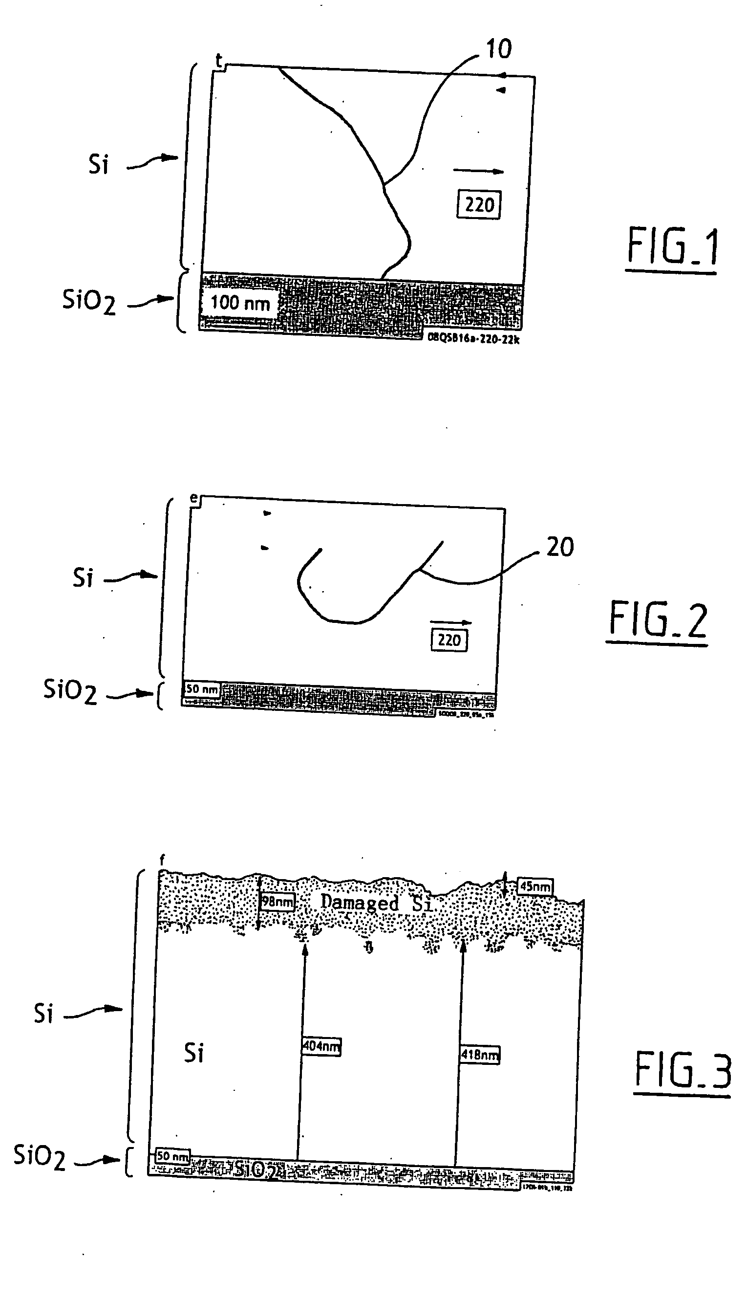
[0042] In order to avoid the generation of such secondary defects and to apply the demonstration of the “starting point” effect mentioned above demonstrated by the Applicant (initial defects in a wafer—for example defects on its disturbed surface—form starting points from which much larger secondary defects are generated during a high temperature heat treatment), the high temperature heat treatment according to the invention is preceded by a surface preparation step of the wafer to be treated.

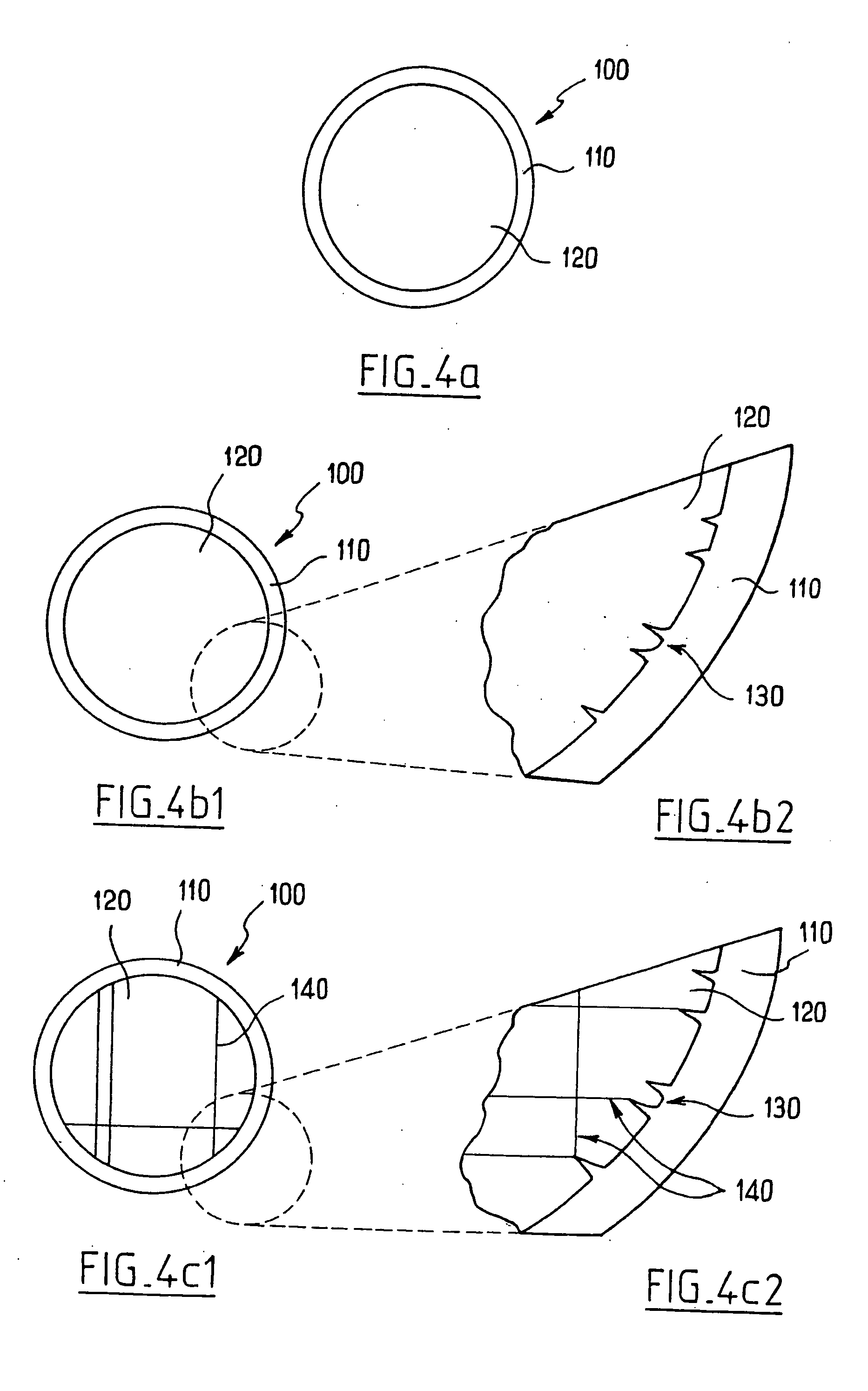
[0043] This preparation corresponds to a thinning step of the s...


PUM

PropertyMeasurementUnit
Temperatureaaaaaaaaaa
Timeaaaaaaaaaa

Abstract

This invention relates to a process for treatment of a multi-layer wafer with materials having differential thermal characteristics, the process comprising a high temperature heat treatment step that can generate secondary defects, characterised in that this process includes a wafer surface preparation step before the high temperature heat treatment step.

Description

TECHNICAL FIELD [0001] This invention relates in general to surface treatment of multi-layer wafers formed from layers of materials chosen from among semiconducting materials. More precisely, the invention relates to a process for treatment of a multi-layer wafer with materials having differential thermal characteristics, as defined herein, with the process comprising a high temperature heat treatment step that can generate secondary defects. BACKGROUND ART [0002] Note that a “wafer” means a structure that may include one or several layers. In the case of a multi-layer wafer, the different layers may have been associated with each other by any type of technique known in itself (layer transfer, gluing, epitaxy, etc.). Thus, a multi-layer wafer is such a structure that contains several layers. And the wafers concerned by this invention are wafers comprising a thin surface layer (made of a material such as silicon) for applications in micro-electronics. Remember that the useful layer i...

Claims


Application Information

Patent Timeline
IPC IPC(8): H01L21/20H01L21/762
CPCH01L21/02032Y10S438/974H01L21/76254H01L21/2007H01L21/20H01L21/324
Inventor RAYSSAC, OLIVIERBLONDEAU, BERYLMORICEAU, HUBERTLAGAHE-BLANCHARD, CHRISTELLEFOURNEL, FRANCK
Owner S O I TEC SILICON ON INSULATOR THECHNOLOGIES
Why Eureka
Try Eureka