Reconfigurable circuit, processor having reconfigurable circuit, method of determining functions of logic circuits in reconfigurable circuit, method of generating circuit, and circuit

a reconfigurable circuit and processor technology, applied in the field of integrated circuit technologies, can solve the problems of large packaging area and high cost of control circuits, complicated wiring patterns among the basic cells, and large packaging area of lsis designs using fpgas, so as to reduce the scale of circuits

Inactive Publication Date: 2005-06-23
SANYO ELECTRIC CO LTD
View PDF5 Cites 229 Cited by
  • Summary
  • Abstract
  • Description
  • Claims
  • Application Information

AI Technical Summary

Benefits of technology

[0008] To solve the foregoing problems, one of the aspects of the present invention provides a reconfigurable circuit comprising: a plurality of groups of logic circuits capable of changing functions; and at least one connection unit arranged between the groups, being capable of establishing connection between the logic circuits of the groups selectively. In this reconfigurable circuit, the connection unit is formed so that the logic circuit of one of the groups is connectable with only some of the logic circuits included in another group. When the connection unit thus imposes a limitation on the connection between the logic circuits, it is possible to reduce the number of wires of the connection unit in terms of hardware and reduce such components as switches. This can reduce the circuit scale and achieve power saving advantageously even from an economical viewpoint.
[0009] Another aspect of the present invention provides a processor comprising: a reconfigurable circuit capable of changing functions; a setting unit which supplies the reconfigurable circuit with configuration information for configuring a desired circuit; and a control unit which controls the setting unit to supply the reconfigurable circuit with configuration information on a plurality of circuits capable of simultaneous execution. According to this processor, circuits capable of parallel processing can be formed on the reconfigurable circuit simultaneously. This allows a reduction in processing time.
[0010] Still another aspect of the present invention provides a processor comprising: a DFG generating unit which generates a data flow graph expressing functions of logic circuits as nodes and the flow of data from input data to output data as connections of the nodes; a configuration information generating unit which generates configuration information based on the data flow graph generated; a reconfigurable circuit capable of changing functions; and a setting unit which supplies the reconfigurable circuit with configuration information for configuring a desired circuit. In this processor, when a node has outputs more than the number of logic circuits possible for the corresponding logic circuit to be connected with, the DFG generating unit may distribute the outputs of the node by duplicating the node into ones having the same inputs in the data flow graph. Consequently, even if nodes cannot be mapped directly on the connection-limited reconfigurable circuit because of an excessive number of connections, the nodes can be duplicated to distribute node outputs, thereby configuring a circuit equivalent to the desired circuit on the reconfigurable circuit.
[0011] Still another aspect of the present invention provides a processor comprising: a DFG generating unit which generates a data flow graph expressing functions of logic circuits as nodes and the flow of data from input data to output data as connections of the nodes; a configuration information generating unit which generates configuration information based on the data flow graph generated; a reconfigurable circuit capable of changing functions; and a setting unit which supplies the reconfigurable circuit with configuration information for configuring a desired circuit. In this processor, when a node has outputs more than the number of logic circuits possible for the corresponding logic circuit to be connected with, the DFG generating unit may distribute the outputs of the node by adding a non-operating through node so as to be in connection with the outputs of the nodes aside from some of output nodes of the node, and arranging the rest of the output nodes after the through node. Consequently, even if nodes cannot be mapped directly on the connection-limited reconfigurable circuit because of an excessive number of connections, through nodes can be arranged to distribute the node outputs, thereby configuring a circuit equivalent to the desired circuit on the reconfigurable circuit.
[0015] According to the present invention, it is possible to provide a reconfigurable circuit of reduced circuit scale, and peripheral technologies thereof.

Problems solved by technology

LSIs designed by using FPGAs, however, have extremely large packaging areas and high costs as compared to when designed by using application specific ICs (ASICs).
The control circuit thus inevitably increases the packaging area.
Moreover, the connections among the basic cells tend to require a complicated wiring pattern with greater wiring lengths, even with a number of switches connected to each of the wires.
Longer delays thus develop from this structure.
On that account, FPGA-based LSIs often remain in prototyping and experimental uses, and are unsuitable for mass production in view of packaging efficiency, performance, cost, etc.
It thus consumes considerable time to configure the circuits.
Consequently, FPGAs are not suited to applications where circuit configuration need to be switched instantaneously.
In this case, however, the capability of passing data to any of the ALUs requires enormous numbers of wires and connection switches, contributing to an increase in circuit scale.

Method used


Image

  • Reconfigurable circuit, processor having reconfigurable circuit, method of determining functions of logic circuits in reconfigurable circuit, method of generating circuit, and circuit
  • Reconfigurable circuit, processor having reconfigurable circuit, method of determining functions of logic circuits in reconfigurable circuit, method of generating circuit, and circuit
  • Reconfigurable circuit, processor having reconfigurable circuit, method of determining functions of logic circuits in reconfigurable circuit, method of generating circuit, and circuit

Examples


first embodiment

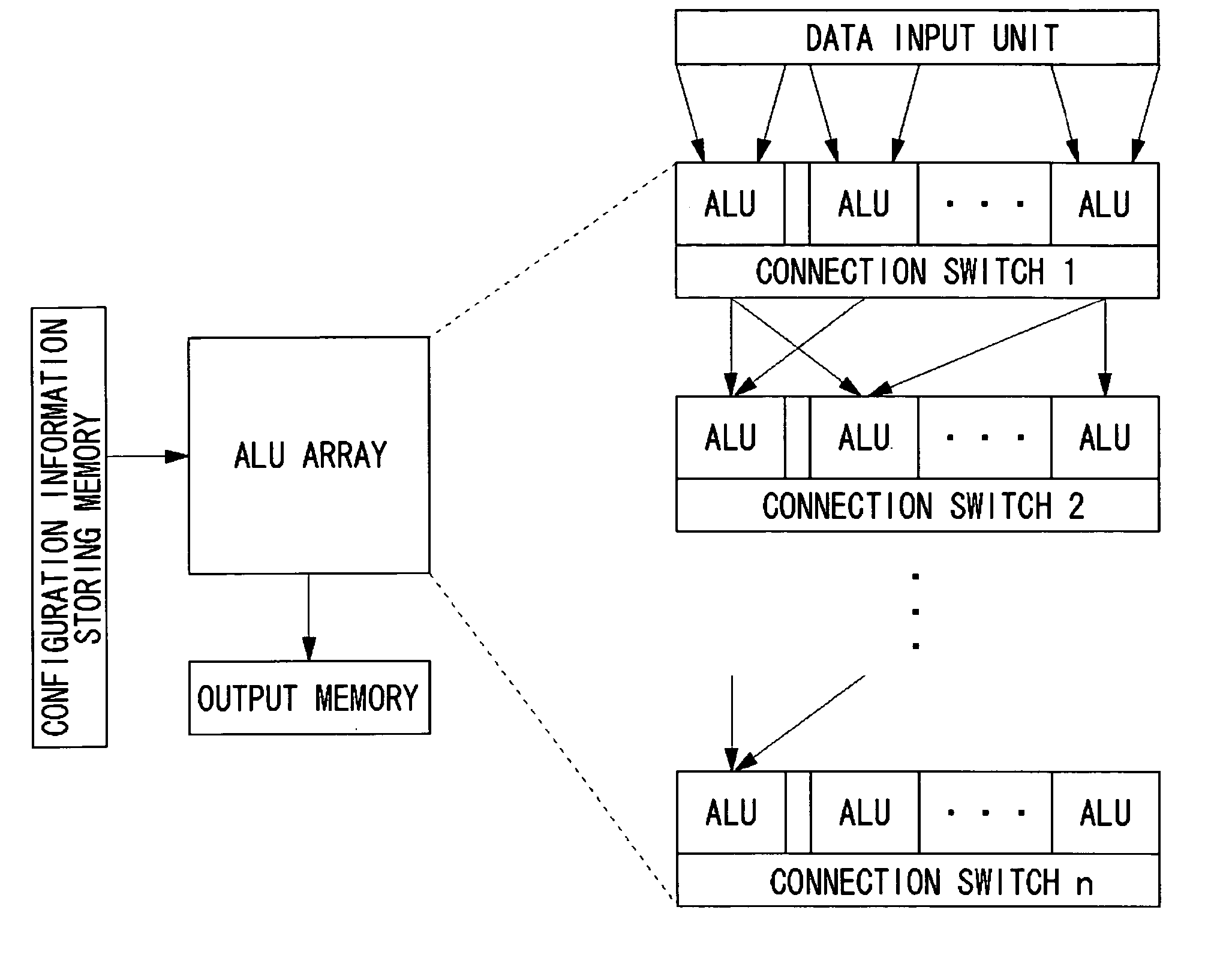
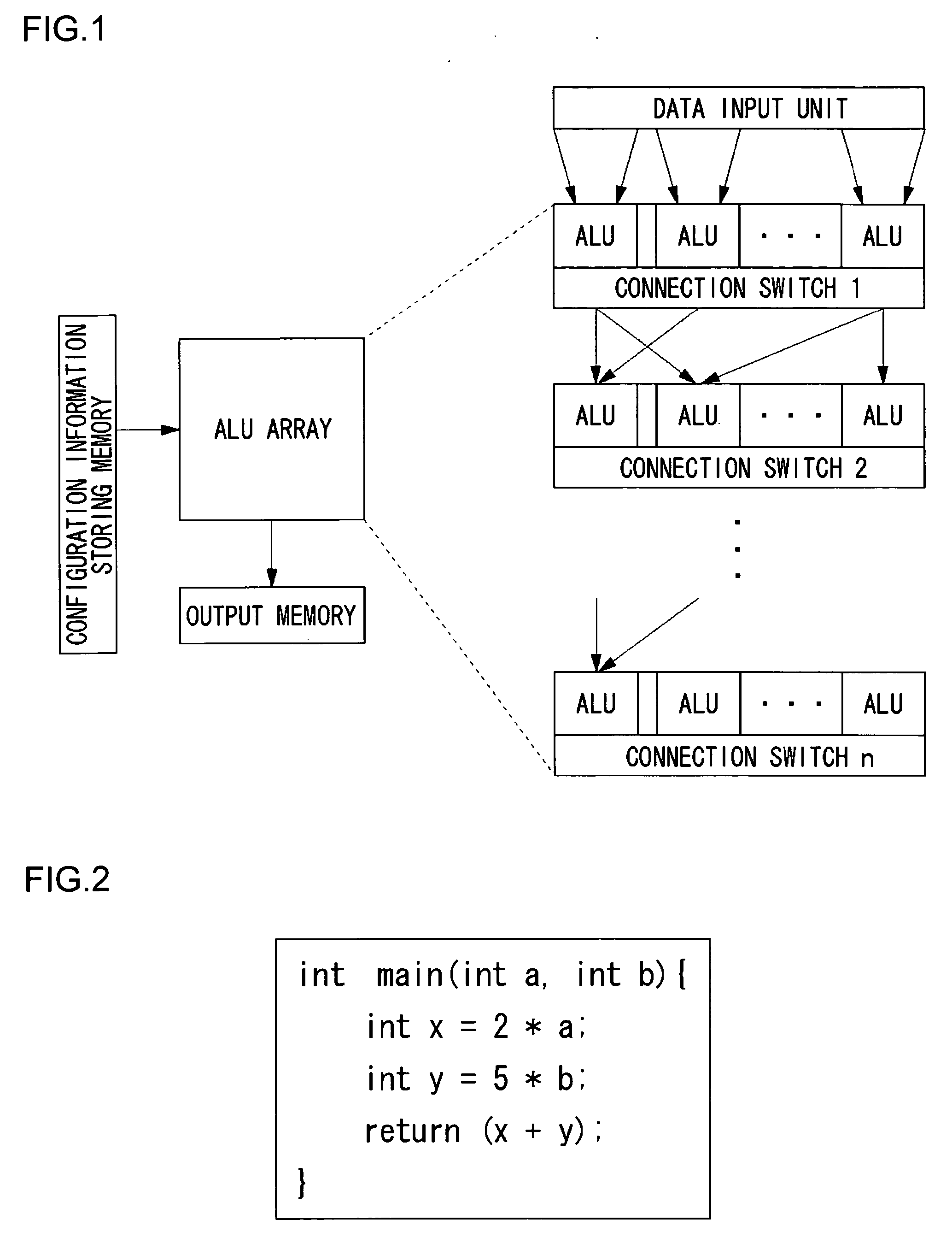
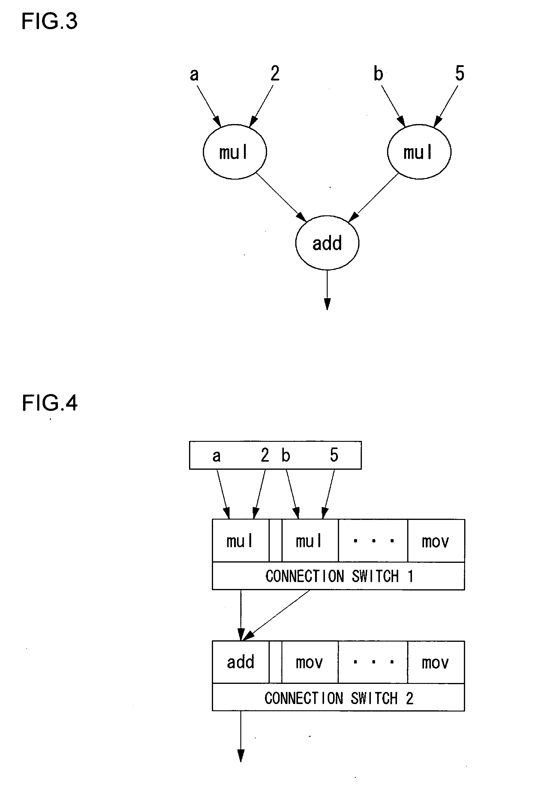
[0064]FIG. 1 is a block diagram showing a reconfigurable processor using an ALU array. As shown in FIG. 1, an instruction set for controlling the functions of ALUs and a connection data set for controlling the connection destinations among the ALUs (hereinafter, referred to as “configuration information”) are initially set to the ALU array from a configuration information storing memory. The ALU array has a plurality of stages, in each of which a plurality of ALUs are arranged. The ALUs have a plurality of arithmetic circuits implemented in advance. Which operations to perform are selected depending on the instruction set. To pass data from ALUs in upper stages to ones in lower stages, connection switches for switching connection among the ALUs are set to the connection data set, whereby which ALUs in the lower stages to pass the data to are determined. During operation, arithmetic processing is performed in accordance with the configuration information, and the results are output. ...

second embodiment

[0067]FIG. 6 is a block diagram showing a processor 10 according to a second embodiment. The processor 10 is provided with an integrated circuit device 26. The integrated circuit device 26 has the facilities of making the circuit configuration reconfigurable. The integrated circuit device 26 is formed on a single chip, and comprises a reconfigurable circuit 12, a setting unit 14, a control unit 18, an internal state holding circuit 20, an output circuit 22, and a path part 24. The reconfigurable circuit 12 allows function changes by changing settings.

[0068] The setting unit 14 has a first setting unit 14a, a second setting unit 14b, a third setting unit 14c, a fourth setting unit 14d, and a selector 16. The setting unit 14 supplies the reconfigurable circuit 12 with configuration information 40 for configuring a desired circuit. The path part 24 functions as a feedback path, connecting the outputs of the reconfigurable circuit 12 to the inputs of the reconfigurable circuit 12. The ...

third embodiment

[0093] The DFG created from the C program of FIG. 2 falls within the size of the ALU array in the reconfigurable circuit 12 (in this case, three rows x six columns). A third embodiment will deal with the processing when the DFG exceeds this ALU array size. When a DFG exceeds the vertical size of the ALU array, the DFG is divided in the vertical direction of the ALU array.

[0094]FIG. 12 shows an example of the virtual state where a DFG exceeding the vertical size of the ALU array is mapped to the ALU array. Since this DFG has a vertical size of 5, the DFG generating unit 30 generates two sub DFGs of divided circuits into which this DFG is divided.

[0095] FIGS. 13(a) and 13(b) show the states where the two sub DFGs into which the DFG of FIG. 12 is divided are mapped to the ALU array. FIG. 13(a) shows the state of mapping of the ALU array for the first three stages shown in FIG. 12. FIG. 13(b) shows the state of mapping of the ALU array for the last two stages shown in FIG. 12. Here, t...


PUM


Abstract

A reconfigurable circuit of reduced circuit scale. The reconfigurable circuit of the present invention comprises a plurality of ALUs capable of changing functions. The plurality of ALUs are arranged in a matrix. At least one connection unit capable of establishing connection between the ALUs selectively is provided between the stages of the ALUs. This connection unit is not intended to allow connection between all the logic circuits in adjoining stages, but is configured so that the logic circuits are each connectable with only some of the logic circuits pertaining to the other stages. The connection limitation allows a reduction in circuit scale.

Description

BACKGROUND OF THE INVENTION [0001] 1. Field of the Invention [0002] The invention relates to integrated circuit technologies, and more particularly to a processor having a reconfigurable circuit, and the like. [0003] 2. Description of the Related Art [0004] Recently, reconfigurable processors capable of changing their hardware operations depending on applications have been under development. Among the architectures for realizing reconfigurable processors are ones using digital signal processors (DSPs) and field programmable gate arrays (FPGAs). [0005] With FPGAs (Field Programmable Gate Arrays), circuit configurations can be designed relatively freely by writing circuit data after the fabrication of the LSIs. FPGAs are used for designing dedicated hardware. An FPGA includes basic cells and programmable wiring resources for linking the basic cells. The basic cells each have a look-up table (LUT) for storing a truth table of the logic circuit, and a flip-flop for output. With FPGAs, i...

Claims


Application Information

Patent Timeline
Patent Type & Authority Applications(United States)
IPC IPC(8): G06F15/78G06F17/50G06F7/00H01L21/82H03K19/173H03K19/177
CPCG06F15/7867H03K19/17728H03K19/17736Y02B60/1225H03K19/1778Y02B60/1207H03K19/17748Y02D10/00
Inventor OKADA, MAKOTOHIRAMATSU, TATSUONAKAJIMA, HIROSHIOZONE, MAKOTO
Owner SANYO ELECTRIC CO LTD
Why Eureka
Try Eureka