
Methods of forming a high germanium concentration silicon germanium alloy by epitaxial lateral overgrowth and structures formed thereby

a technology of germanium germanium alloy and epitaxial overgrowth, which is applied in the direction of crystal growth process, transistor, chemistry apparatus and process, etc., can solve the problems of limited purification of silicon photodetectors, forming in silicon-germanium films, and detecting wavelengths

Inactive Publication Date: 2005-06-23
INTEL CORP
View PDF5 Cites 70 Cited by
  • Summary
  • Abstract
  • Description
  • Claims
  • Application Information

AI Technical Summary

Problems solved by technology

Pure silicon photodetectors are limited in that they can only detect wavelengths up to about 1 micron.
However, adding germanium to the silicon film often results in a strain to the silicon crystal lattice that may causes defects, such as threading dislocations, to be formed in the silicon-germanium film.
The proliferation of such defects can result in an increase in the defect concentration, or defect density, in the silicon germanium film, which can impair the performance of a silicon germanium photodetector device.

Method used


Image

  • Methods of forming a high germanium concentration silicon germanium alloy by epitaxial lateral overgrowth and structures formed thereby
  • Methods of forming a high germanium concentration silicon germanium alloy by epitaxial lateral overgrowth and structures formed thereby
  • Methods of forming a high germanium concentration silicon germanium alloy by epitaxial lateral overgrowth and structures formed thereby

Examples


Embodiment Construction

[0010] In the following detailed description, reference is made to the accompanying drawings that show, by way of illustration, specific embodiments in which the invention may be practiced. These embodiments are described in sufficient detail to enable those skilled in the art to practice the invention. It is to be understood that the various embodiments of the invention, although different, are not necessarily mutually exclusive. For example, a particular feature, structure, or characteristic described herein, in connection with one embodiment, may be implemented within other embodiments without departing from the spirit and scope of the invention. In addition, it is to be understood that the location or arrangement of individual elements within each disclosed embodiment may be modified without departing from the spirit and scope of the invention. The following detailed description is, therefore, not to be taken in a limiting sense, and the scope of the present invention is defined...


PUM


Abstract

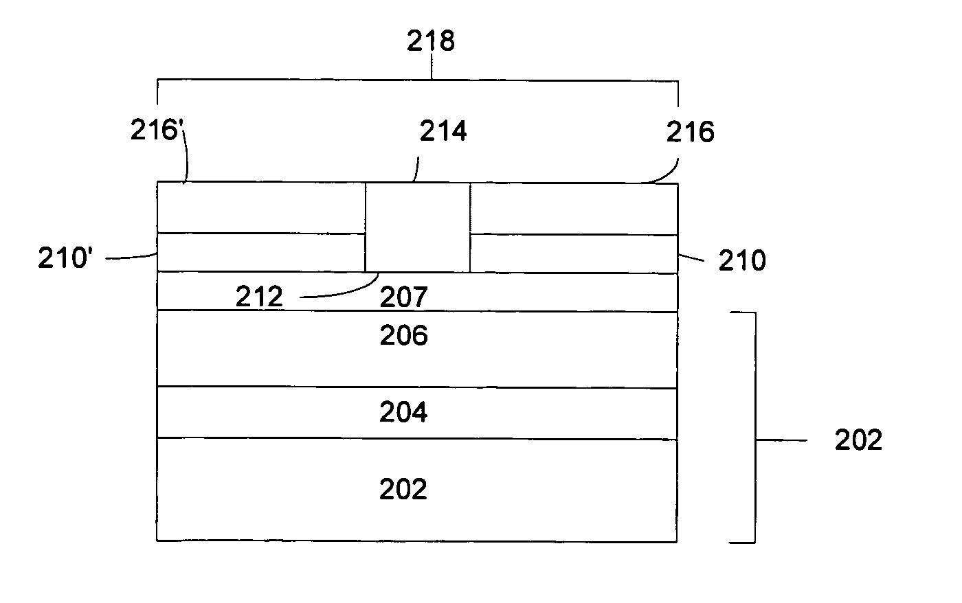
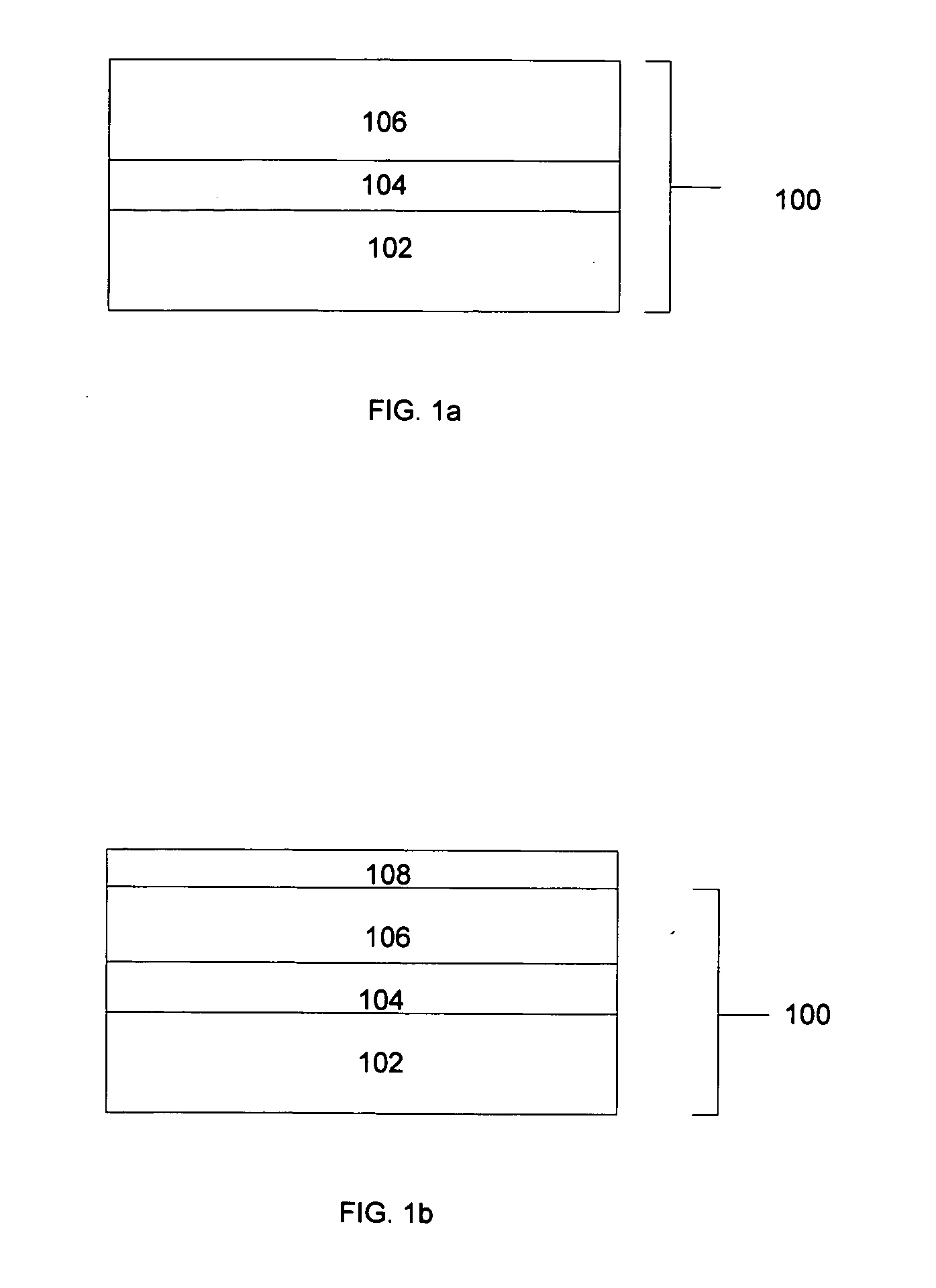
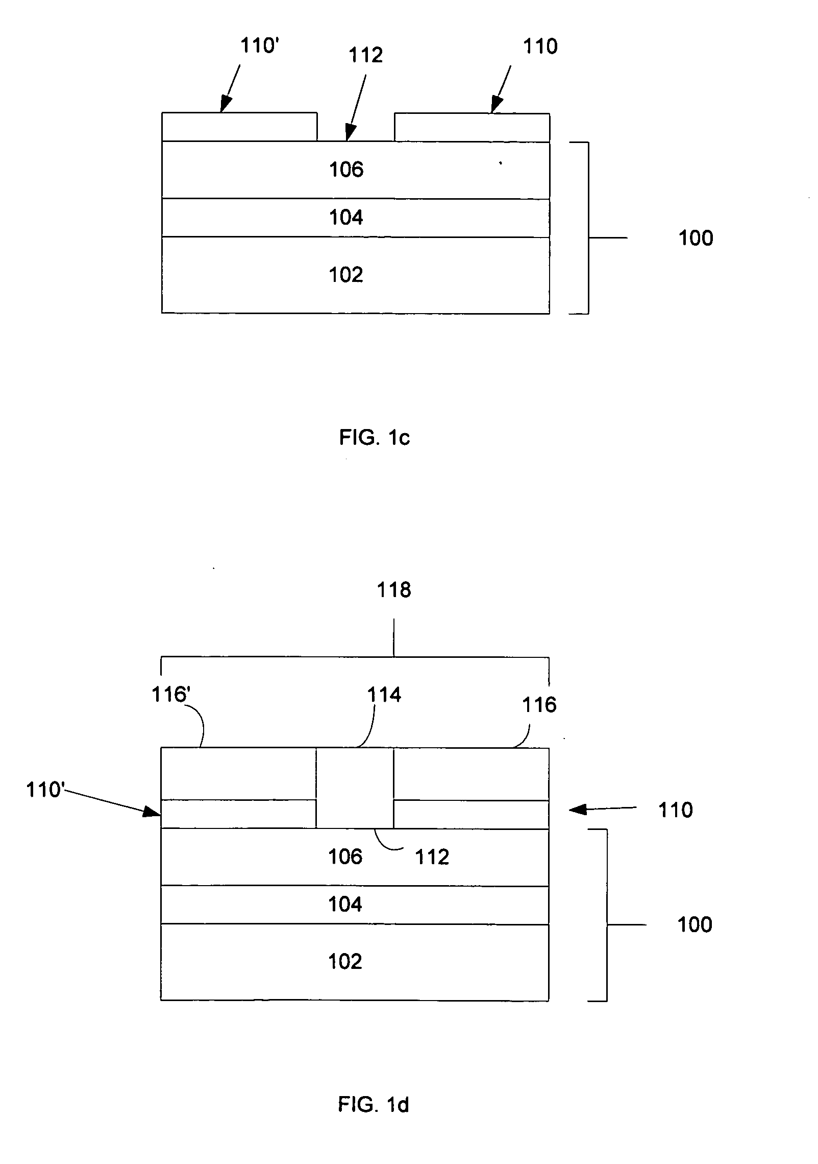
A method of forming a high germanium concentration, low defect density silicon germanium film and its associated structures is described, comprising forming a dielectric layer on a substrate, patterning the dielectric layer to form a silicon region and at least one dielectric region, and forming a low defect silicon germanium layer on at least one dielectric region.

Description

FIELD OF THE INVENTION [0001] The present invention relates to the field of semiconductor processing, and more particularly to methods of processing germanium layers for use in microelectronic photo detectors and structures formed thereby. BACKGROUND OF THE INVENTION [0002] High speed infrared photodetectors are becoming increasingly important for optical communication signal processing, infrared imaging and measurement systems. Photodetectors can be used for the detection of optical communication signals, such as those used in the telecommunication industry. A standard wavelength used in the telecommunication industry is 1.3 microns. Pure silicon photodetectors are limited in that they can only detect wavelengths up to about 1 micron. The addition of germanium to a silicon film used to fabricate a photodetector can increase the wavelength that can be detected (i.e., photodetector responsivity). For example, using a silicon-germanium film which incorporates more than 50 percent germ...

Claims


Application Information

Patent Timeline
IPC IPC(8): H01L21/20H01L21/762H01L29/786H01L31/105H01L31/18
CPCH01L21/02381H01L21/0245H01L21/02532H01L21/02639H01L21/02647Y02E10/50H01L29/78609H01L29/78687H01L31/105H01L31/1812H01L21/76262Y02E10/548
Inventor MORSE, MIKE
Owner INTEL CORP
Learn More