Process for Growth of Low Dislocation Density Gan

a technology of dislocation density and growth process, which is applied in the direction of crystal growth process, polycrystalline material growth, chemically reactive gas growth process, etc., can solve the problems of low defect density, affecting the growth of low-defect density iii-n layers, and affecting the development of nitride materials, etc., to achieve the effect of low defect density

Active Publication Date: 2009-11-12
IV WORKS
View PDF17 Cites 25 Cited by
  • Summary
  • Abstract
  • Description
  • Claims
  • Application Information

AI Technical Summary

Benefits of technology

[0026]An object of the present invention is to provide a method of manufacturing thick GaN substrates having an extremely low defect density and little warp and bow by the ULO process without using any kind of mask, nor roughening, nor etching, nor grooving the GaN surface, and only by changing the operating pressure in the growth chamber, the partial pressure, the temperature, the V / III ratio and / or by the addition of surfactant or antisurfactant chemical species in the vapour phase.

Problems solved by technology

Unfortunately, the development of nitride materials has been hampered by problems in the processing technology of such materials.
One of the most important problems in the development of III-N devices is the lack of gallium nitride bulk substrates of acceptable usable area or of lattice-matched substrates for growth of low-defect density III-N layers.
Substantial difficulties have been shown when attempting to obtain large-area crystals of any Group III-nitride that could provide suitable substrates for device fabrication.
This technology has been developed previously, but the size of the substrate (˜1 cm2) and the volume of the potential mass production do not reach by far the industrial needs.
The techniques currently used for the fabrication of relatively high quality GaN and related layers involve the heteroepitaxial deposition of a GaN device layer onto a suitable but non-ideal substrate.
All heteroepitaxial substrates present challenges to the high-quality deposition of GaN, in the form of lattice and thermal mismatch.
Thermal mismatch is caused by differences in the thermal expansion coefficient between dissimilar materials.
However, even this method cannot compensate the lattice-mismatch between the substrate and the crystal, and the GaN film has still numerous defects.
Such large mismatches lead to the formation of very high densities of threading dislocations (TD) (˜109 cm−2) and eventually cracks.
Typically, after the GaN is grown, as the sample cools to room temperature, the difference in thermal expansion (contraction) rates gives rise to high levels of stress at the interface between the two materials.
Above a film thickness of about 10 microns, the stress levels exceed the fracture limits of the GaN, and cracking of the film may result.
Cracks in this layer are even less desirable than high dislocation densities since they may propagate during the processing of device structure.
The existence of extended defects (threading dislocations, stacking faults, and antiphase boundaries) leads to significantly deteriorated performances and results in a shortened operating lifetime of devices.
More specifically, the dislocations behave as nonradiative centres, thus reducing the light-emitting efficiency of light-emitting diodes and laser diodes made from these materials.
Although threading dislocations have not prevented the development of high-brightness light-emitting diodes, the dislocations cause excessive reverse-bias leakage currents in p-n junction devices such as high-electron-mobility transistors, field-effect transistors and other electronic devices.
Further, the dislocations can act as strong scattering centres for carriers, thus reducing the mobility of electrons and holes, limiting the performance of many semiconductor devices.
Because HVPE was unable to produce p-type GaN, it was largely abandoned in the early 1980s.
As the layer becomes thicker, this leaves primarily edge dislocations with larger separation, therefore interactions become less and less likely and a further decrease of the density of TDs becomes difficult.
ELO technologies have also been implemented in HVPE, but due to the high growth rate, wide pitch of the ELO openings in masks are required and new dislocations are often generated.

Method used


Image

  • Process for Growth of Low Dislocation Density Gan
  • Process for Growth of Low Dislocation Density Gan
  • Process for Growth of Low Dislocation Density Gan

Examples


example 1

Growth of GaN / Sapphire Template with ELO Quality by MOVPE

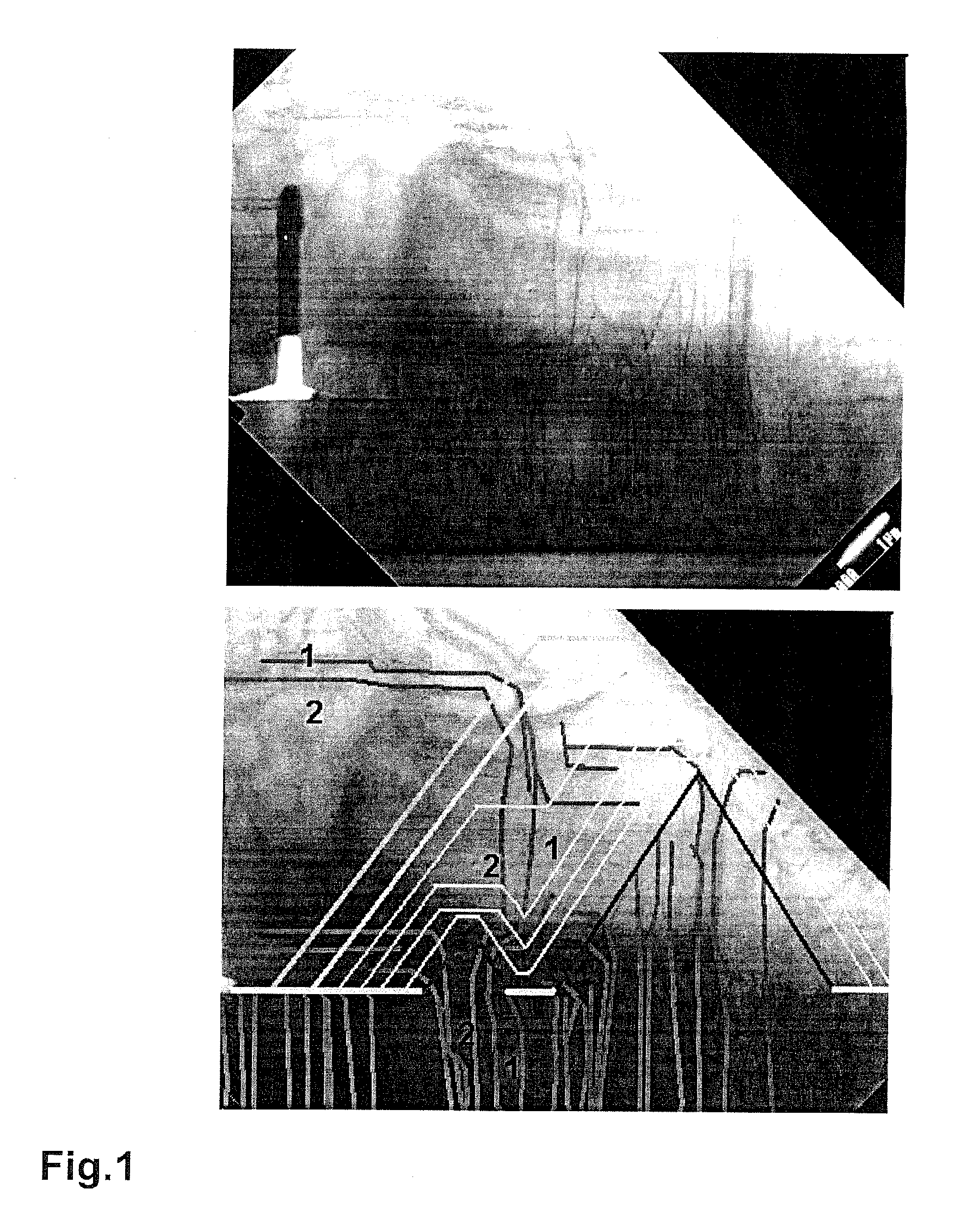
[0081]A (0001) sapphire substrate is used. A very thin film of silicon nitride is formed on the surface of the sapphire, the film being obtained by reaction between NH3 and silane SiH4 for a time short enough to limit the thickness of the film to that of about a few mono layers.

[0082]The gaseous vehicle is a mixture of nitrogen and hydrogen in equal proportions. The ammonia is introduced together with the silane, in a form diluted to 50 ppm in hydrogen. Under these conditions, the typical NH3 and SiH4 reaction time is of the order of 30 seconds. This reaction time could be increased up to 360 seconds. This creates either a continuous SiN layer (reaction time 60 seconds) or a discontinuous SiN layer with nanoholes of random size (deposition time 360 seconds)

[0083]The successive steps are monitored by laser reflectometry (LR). After the SiN layer coating, a continuous gallium nitride layer having a thickness of 20 to 30 nm is de...

example 2

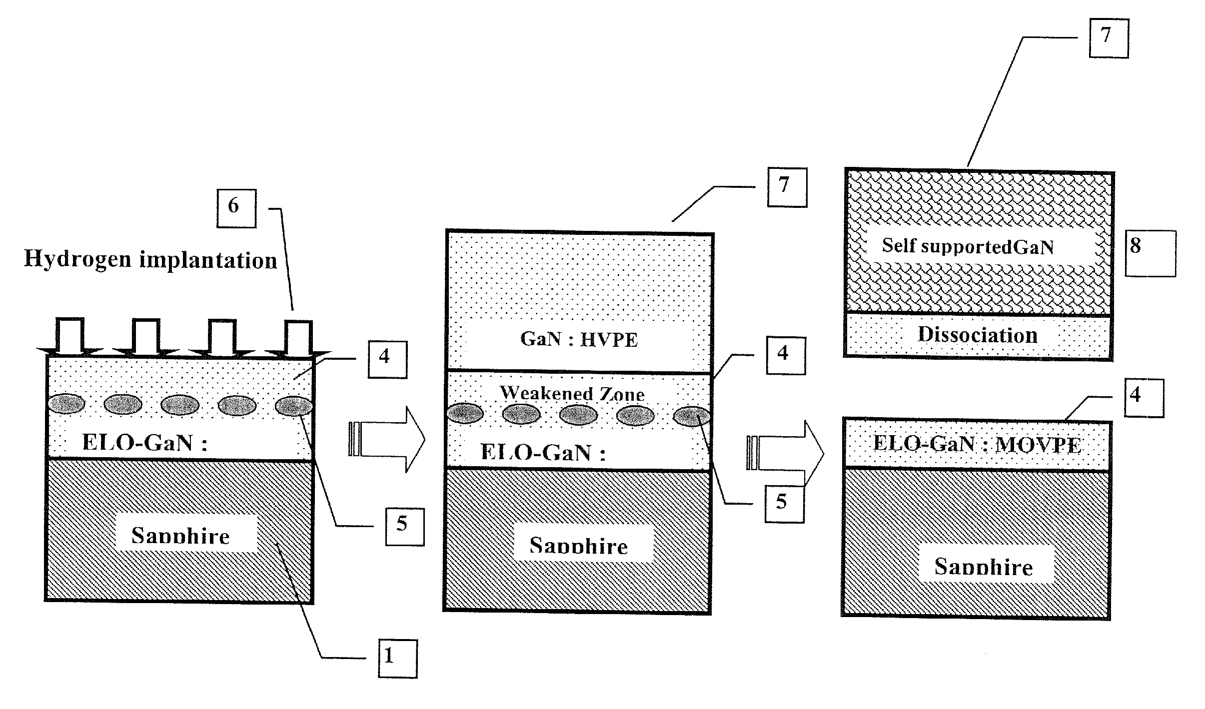
Formation of a Free Standing GaN

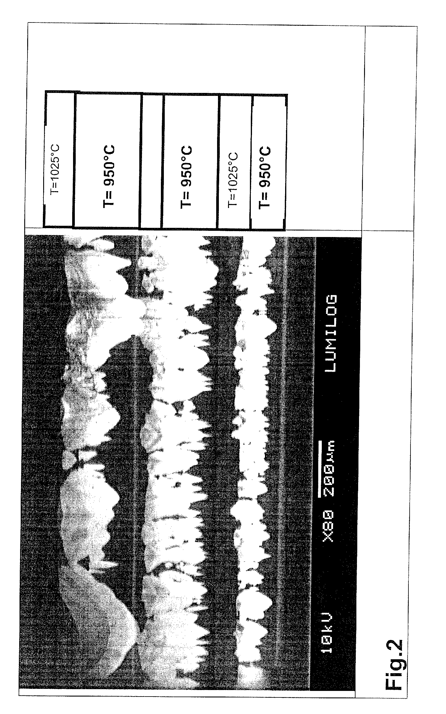
[0085]Using the GaN / sapphire templates of example 1, the HVPE growth starts at about 950° C. In this low temperature step of growing a thick GaN layer by HVPE, the temperature is set at 930-950° C., the partial pressure of HCl, pHCl at 0.03, of NH3, pNH3 at 0.24, the carrier gas, H2, pH2 at 0.73 respectively. The growing pressure was 2.6 kPa.

[0086]After the low temperature step, formation of islands, growth temperature is set up to 1025° C., with the following values for the partial pressures of active and carrier gas:[0087]pHCl, 0.02[0088]PNH3, 0.31[0089]pH2, 0.67[0090]Working pressure: 2.6 kPa

[0091]In these growth conditions, the lateral growth rate is enhanced and the layer becomes flat. CL corresponding to this high temperature growth step appears as grey, because of the high quality of the GaN layer and the reduced incorporation of Oxygen.

[0092]The process is repeated several times until a thickness of 500 μm to 2 mm is obtained. CL examination o...

example 3

[0099]In this example, three alternate low-high growth temperature growth processes with different temperatures and durations are used. More specifically, it is shown that cross sectional optoelectronic properties of the HVPE layer are linked to the growth process.

[0100]The GaN / sapphire templates of example 1, is hereafter introduced in the growth chamber of the HVPE reactor.

[0101]The HVPE growth starts at about 930° C. In this low temperature step of growing a thick GaN layer by HVPE, the partial pressure of HCl, pHCl at 0.03, of NH3, pNH3 at 0.24, the carrier gas, H2, pH2 at 0.73 respectively. The growing pressure was 2.6 kPa. At this rather low temperature, GaN grows in the form of coherent island, randomly distributed with random size, thus involving a ULO process.

[0102]After the low temperature step, growth temperature is set up to 1015-1020° C., with the following values for the partial pressures of active and carrier gas:[0103]pHCl, 0.02[0104]PNH3, 0.31[0105]pH2, 0.67[0106]Wo...


PUM


Abstract

High quality free standing GaN is obtained using a new modification of the Epitaxial Lateral Overgrowth technology in which 3D islands or features are created only by tuning the growth parameters. Smoothing these islands (2D growth) is achieved thereafter by setting growth conditions producing enhanced lateral growth. The repetition of 3D-2D growth results in multiple bending of the threading dislocations thus producing thick layers or free standing GaN with threading dislocation density below 106 cm−2.

Description

FIELD OF THE INVENTION[0001]The invention relates to a process for growth of low dislocation density GaN on a substrate, and more particularly, to a process for epitaxial growth where the lateral and vertical growth rates of the material are controlled only by growth conditions. It also relates to a nitride semiconductor wafer having a GaN crystal formed by such a method and a nitride semiconductor device produced there from.DESCRIPTION OF THE RELATED ART[0002]GaN-based compound semiconductors, such as gallium nitride (GaN), the ternary alloys, indium gallium nitride (InGaN) and gallium aluminium nitride (GaAlN) and even the quaternary (AlGaInN) are direct band gap semiconductors. Their band gaps cover wavelengths extending from visible to UV. Henceforth, nitride alloy semiconductors are recognized as having great potential for short wave length emission. GaN is used in the manufacture of light emitting diodes (LEDs), blue-violet laser diodes (LDs) and UV detectors. The next generat...

Claims


Application Information

Patent Timeline
Patent Type & Authority Applications(United States)
IPC IPC(8): H01L29/20H01L21/20
CPCC30B25/02C30B29/40C30B29/406H01L21/0237H01L21/02647H01L21/02458H01L21/0254H01L21/0262H01L21/02639H01L21/0242C30B29/38H01L21/20
Inventor BEAUMONT, BERNARDFAURIE, JEAN-PIERREGIBART, PIERRE
Owner IV WORKS
Why Eureka
Try Eureka