Non-adhesive semiconductor wafer holder and assembly

a technology of semiconductor wafers and holder plates, applied in the field of non-adhesive semiconductor wafer holders, can solve the problems of high cost of semiconductor processing and inspection, number of wafers, etc., and achieve the effect of reducing the risk of high potential damage at mounting, avoiding high potential damage, and more expensive handling systems

Inactive Publication Date: 2005-06-23
TEXAS INSTR INC
View PDF6 Cites 4 Cited by
  • Summary
  • Abstract
  • Description
  • Claims
  • Application Information

AI Technical Summary

Benefits of technology

[0006] Handling time of a semiconductor wafer using the present invention cuts about 10 minutes off the process time per wafer when processed individually, and cuts about 5 minutes per wafer when processing more than one wafer. This wafer holder and process eliminates the need for more expensive handling systems which is a significant cost

Problems solved by technology

Semiconductor processing and inspection is an expensive process, and the throughput time for the processing and

Method used


Image

  • Non-adhesive semiconductor wafer holder and assembly
  • Non-adhesive semiconductor wafer holder and assembly
  • Non-adhesive semiconductor wafer holder and assembly

Examples


Embodiment Construction

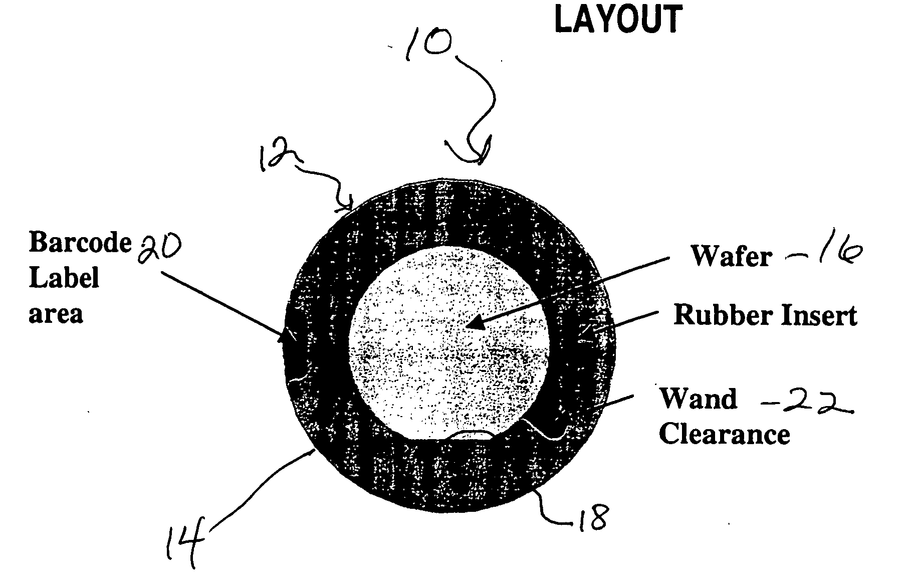
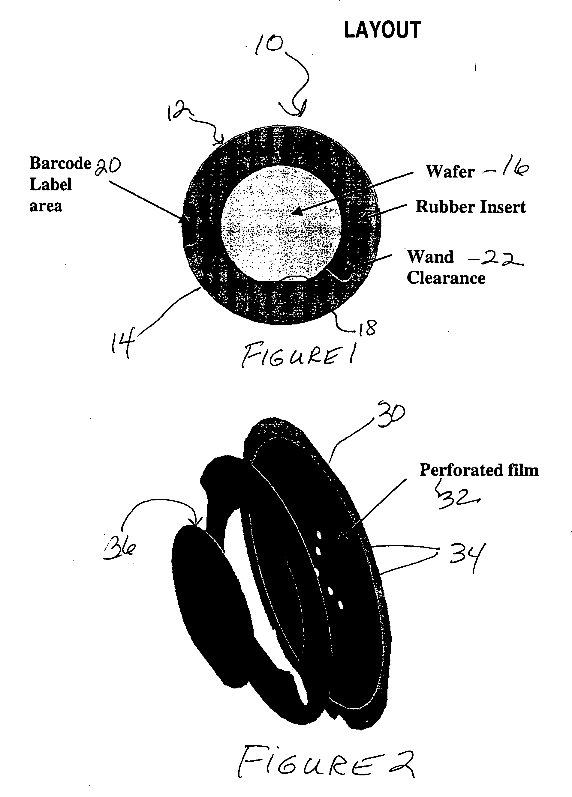
[0010] Referring now to FIG. 1, there is generally shown at 10 a top view of a layout of the present invention seen to comprise a semiconductor wafer holder 12. Wafer holder 12 has a concentric opening 14 having a size and profile adapted to securely engage the edge of a semiconductor wafer 16. The wafer holder 12 is seen to be generally circular, wherein opening 14 has a profile including a flat edge 18 that conforms to the flat edge of the semiconductor wafer 16. The wafer holder 12 is preferably comprised of a resilient material such as a rubber insert and comprised of a silicon foam material, to provide a resilient edge defining opening 14. Of course, other resilient materials are suitable which are resilient to securingly engage the perimeter of the semiconductor wafer 14 in an interference fit, and without damage thereto. The wafer holder 12 may also include a bar code label area 20, and a wand clearance 22.

[0011] Referring now to FIG. 2, there is shown an exploded view of th...


PUM


Abstract

A semiconductor wafer holder (12) and process eliminating the need for wafer mounting using sticky tape, UV exposure, and manual de-taping from sticky tape during processing and inspection. The present invention comprises a semiconductor holder having an opening (14) securely receiving a semiconductor wafer (16) about its edges in an interference fit. The holder securely holds the wafer in place during handling, and without the need for using sticky tape to hold the wafer backside to a wafer tray (30). The wafer holder is utilized as an insert that is concentric to the wafer tray, which tray includes a perforated film (32) having vacuum openings (34). Advantageously, sticky tape is only interposed between the wafer holder (12) and a perimiter of the wafer holder (30), which sticky tape is later removed using UV exposure.

Description

FIELD OF THE INVENTION [0001] The present invention is generally related to semiconductor wafer processing handling systems, and more particularly to devices and methods used for processing semiconductor wafers in a film frame assembly. BACKGROUND OF THE INVENTION [0002] Conventional semiconductor wafer handling systems typically utilize semiconductor trays to carry a semiconductor wafer during processing and during inspection of the wafer after processing. Conventionally, a sticky tape is utilized to secure a bottom surface of the semiconductor wafer to the wafer tray during this processing and inspection process. After wafer processing and inspection, the sticky film is exposed to a UV light to remove the sticky tape and adhesive. The semiconductor wafer is thereafter handled using a vacuum coupled to the wafer bottom surface. [0003] Semiconductor processing and inspection is an expensive process, and the throughput time for the processing and inspection attributable to handling r...

Claims


Application Information

Patent Timeline
IPC IPC(8): H01L21/4763H01L21/673H01L21/687
CPCH01L21/68785H01L21/67346
Inventor RAMIREZ, JOSE GOVEAGRAHAM, ROBERT O.
Owner TEXAS INSTR INC
Why Eureka
Try Eureka