Wireless transceiver for automotive vehicle
a transceiver and automotive technology, applied in the field of wireless transceivers, can solve the problems of circuit board bending with the impact, transceiver damage, contact portion between an electronic part and a circuit board in the transceiver may be cracked by an impact, etc., and achieve the effect of high impact resistance and high water resistan
- Summary
- Abstract
- Description
- Claims
- Application Information
AI Technical Summary
Benefits of technology
Problems solved by technology
Method used
Image

Examples
first embodiment
[0023] (First Embodiment)
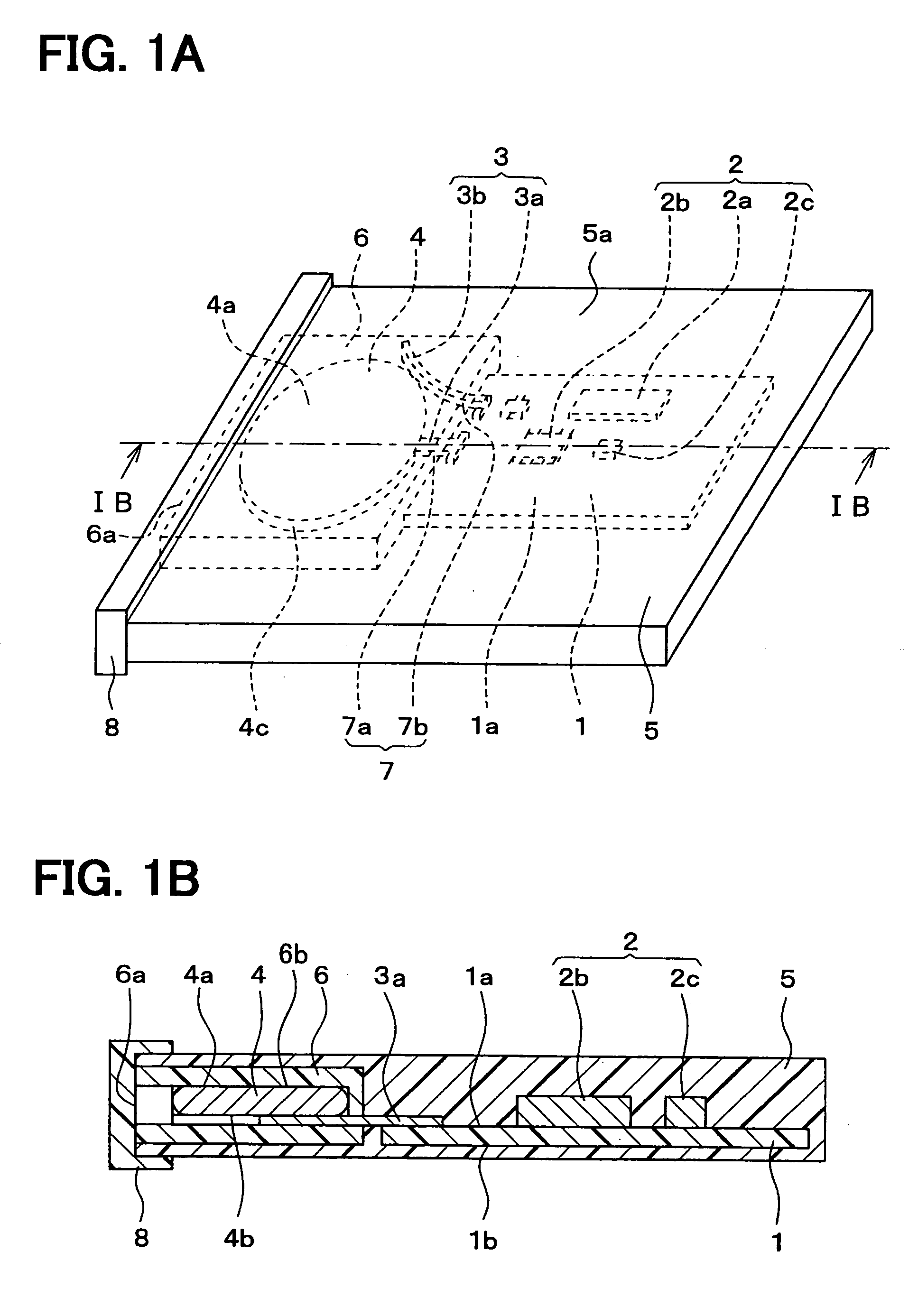
[0024] The inventors have preliminarily studied about a card type transceiver shown in FIGS. 11A and 11B. The transceiver includes a circuit board 12 and a casing 13, which is composed of an upper casing 13a and a lower casing 13b. A circuit part 11 such as an IC chip is mounted on the circuit board 12. The circuit board 12 is sandwiched between the upper and lower casings 13a, 13b so that the circuit board 12 is packaged. The transceiver has a space disposed between the circuit part 11 and the upper casing 13a so that the transceiver has a hollow construction.
[0025] In the above transceiver, if a clearance or a through hole is generated between the upper casing 13a and the lower casing 13b, water may penetrate into the transceiver through the clearance or the through hole. Thus, the transceiver may be damaged.
[0026] Since the transceiver has the hollow construction, when a user of the transceiver drops down the transceiver, a contact portion 14 between th...
second embodiment
[0051] (Second Embodiment)
[0052] A transceiver according to a second embodiment of the present invention is shown in FIGS. 7A and 7B. Further, a method for manufacturing the transceiver is also shown in FIGS. 8A and 8B.
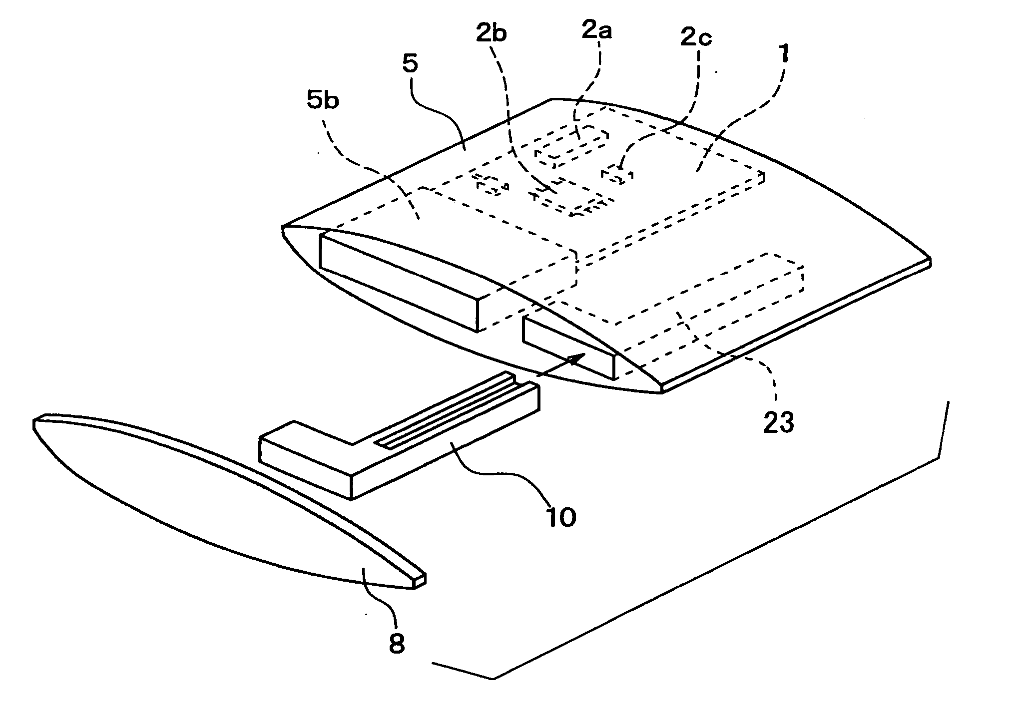
[0053] Although the transceiver shown in FIGS. 1A and 1B has the card type rectangular body, the transceiver in FIGS. 7A and 7B has a different shape. The resin mold 5 becomes thinner as it goes to a side of the transceiver. Therefore, a center portion of the transceiver taken along line VIIB-VIIB in FIG. 7A is the thickest portion. A side portion, for example, shown as line VIIA-VIIA is thinner than the center portion.
[0054] Since the transceiver in FIGS. 7A and 7B has the resin mold 5 with the above described shape in FIGS. 7A and 7B, the user can put the transceiver in his purse easily. Thus, the portability of the transceiver is increased. Further, the total thickness of the transceiver in FIG. 7A is thinner than that of the transceiver in FIG. 1A in a case wher...
third embodiment
[0056] (Third Embodiment)
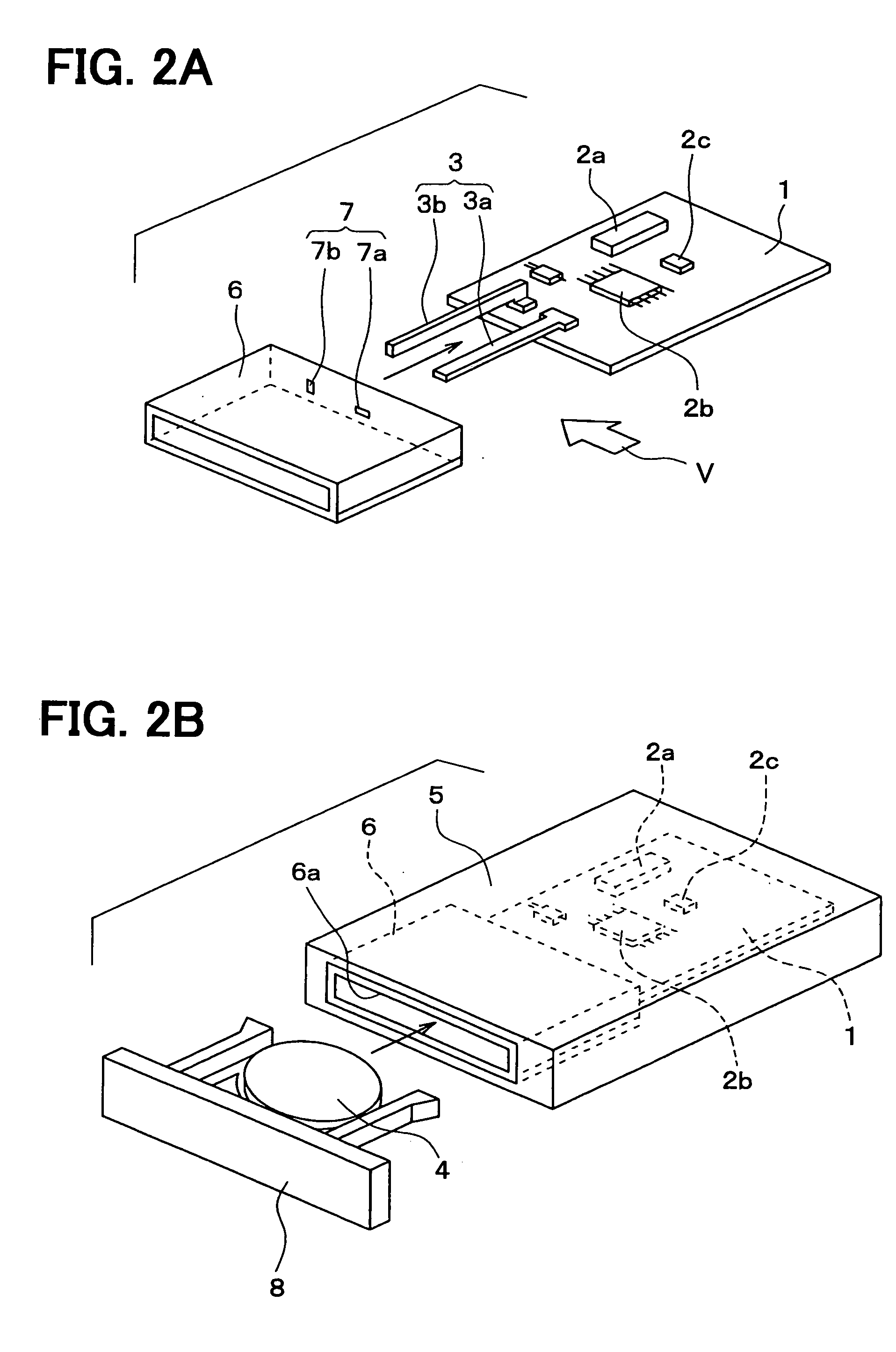
[0057] Although the circuit board 1 and the circuit part 2 is set in the die so that they are molded with the resin mold 5, they can be molded by another method.
[0058] A method for manufacturing the transceiver according to a third embodiment of the present invention is shown in FIG. 9. Firstly, a thin film bag 22 is prepared. The circuit board 1 and the circuit part 2 are inserted into the bag 22. Then, the inside of the film bag 22 is molded with resin by a potting method or the like. Thus, the circuit board 1 and the circuit part 2 are sealed with the resin mold 5.
PUM
 Abstract
Description
Claims
Application Information
 - Generate Ideas
- Intellectual Property
- Life Sciences
- Materials
- Tech Scout
- Unparalleled Data Quality
- Higher Quality Content
- 60% Fewer Hallucinations
Browse by: Latest US Patents, China's latest patents, Technical Efficacy Thesaurus, Application Domain, Technology Topic, Popular Technical Reports.
© 2025 PatSnap. All rights reserved.Legal|Privacy policy|Modern Slavery Act Transparency Statement|Sitemap|About US| Contact US: help@patsnap.com