Wire bonder for ball bonding insulated wire and method of using same

a technology of insulated wire and wire bonding, which is applied in the direction of soldering apparatus, manufacturing tools,auxillary welding devices, etc., can solve the problems of reducing the speed and efficiency of the assembled device, too difficult to manipulate the wire directly during the manufacturing process, and relatively large gaps between wires, etc., to achieve easy integration into existing equipment, easy installation, and low cost

Inactive Publication Date: 2005-06-30
MICROBONDS INC
View PDF20 Cites 4 Cited by
  • Summary
  • Abstract
  • Description
  • Claims
  • Application Information

AI Technical Summary

Benefits of technology

[0009] What is desired according to the present invention is a bonding apparatus and method for effectively bonding insulated wire to a surface which does not damage the wire remote from the bond point. The device and method should be compatible with existing equipment so as to be easy to integrate into existing equipment. In this way there is no need for a completely new bonding device, but merely an upgrade kit of components. Such an apparatus would therefore be easy to install and relatively inexpensive to produce yet would provide secure bonding results for insulated wire. Further the solution must overcome the restricted space available at the bond head of a micro wire bonder.

Problems solved by technology

Typically, the chips are so small and fragile that it is too difficult to manipulate them directly during a manufacturing process.
However, the use of uninsulated wires means relatively large gaps between wires and places constraints upon the bond wire pattern to avoid short circuits.
The requirement for such large gaps frustrates miniaturization and yields unnecessarily long circuit paths which reduce the speed and efficiency of the assembled device.
However, insulated wires cannot be bonded in the usual way.
This leads to damaged wire which cannot be used.
A difficulty to overcome is the very restricted space available at the bond head to deal with the ground issue.

Method used


Image

  • Wire bonder for ball bonding insulated wire and method of using same
  • Wire bonder for ball bonding insulated wire and method of using same
  • Wire bonder for ball bonding insulated wire and method of using same

Examples


Embodiment Construction

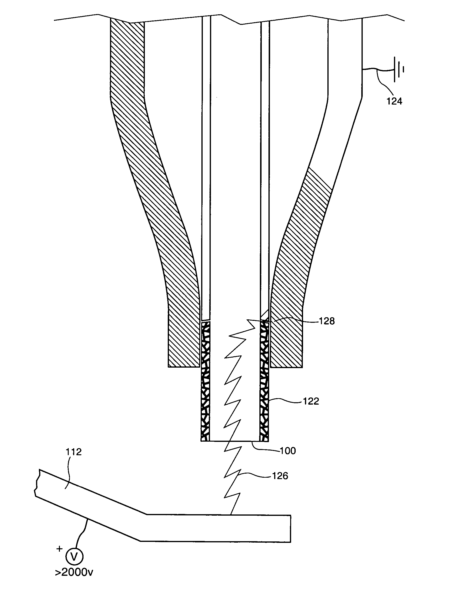
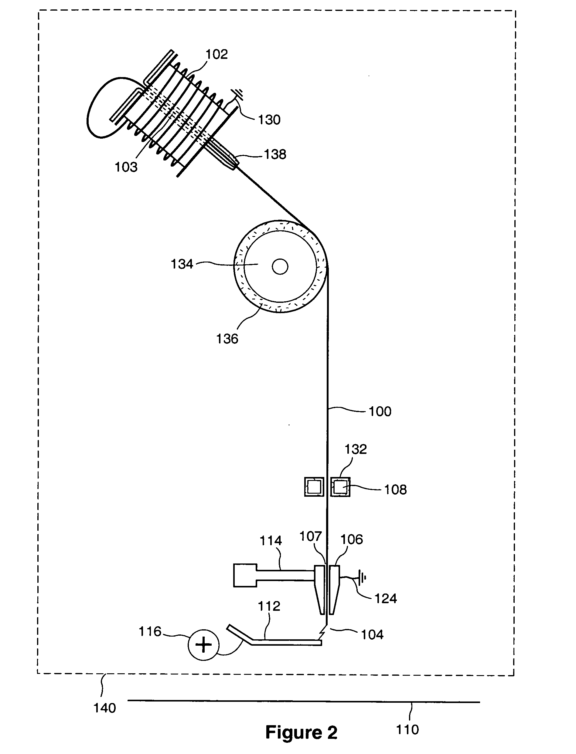
[0051]FIG. 2 shows the elements of the present invention. In a wire bonder enclosed in a casing or housing 140, insulated bond wire 100 is shown extending from a spool 102 remote from a free end 104. The spool acts as a source of insulated wire for the bonder of the present invention. The wire 100 wraps around the spool 102, and is pulled off the spool and through an internal core 103 to supply the micro wire needed to form the wire bonds. The wire 100 is a fine insulated bond wire typically sized 2 mils or less in diameter and made of gold, copper, aluminium, or other conductive material, with 1 mil gold wire being preferred.

[0052] A conductive or metal capillary 106 is also shown having a central bore or tube 107, through which the wire 100 is fed. The capillary 106 acts as a wire holder during the formation of a ball for ball bonding. Although many types of material may be used for the capillary, due to an advantageous combination of strength, conductivity, and ease of manufactu...


PUM

PropertyMeasurementUnit
diameteraaaaaaaaaa
diameteraaaaaaaaaa
discharge voltageaaaaaaaaaa

Abstract

A microchip wire bonder for bonding insulated bond wire to a surface, the microchip wire bonder comprising: a) a body having a stationary electrical contact configured to receive an electrical potential; b) a bond head attached to the body, to position the insulated bond wire adjacent to the surface; c) a rotating wire spooler attached to the body, to hold the insulated bond wire and to advance the insulated bond wire from the spooler to the bond head as needed; and d) an electrical contact device comprising: i) a rotating electrical connector fixed to the rotating wire spooler and being sized and shaped to receive an electrical connection with an uninsulated portion of the insulated bond wire at one end, and having a moving electrical contact at the other end, the two ends being electrically connected; and ii) a conductive bearing configured to electrically couple the moving electrical contact of the electrical connector and the stationary electrical contact; wherein, upon connecting the stationary electrical contact to an electrical potential, and upon connecting the bond wire to the electrical connector, the insulated bond wire will acquire the electrical potential.

Description

CROSS-REFERENCE TO RELATED APPLICATION [0001] This application is a continuation-in-part of U.S. Ser. No. 10 / 300,416, filed on Nov. 20, 2002, the contents all of which are incorporated herein by reference.FIELD OF THE INVENTION [0002] This invention relates generally to the field of bonding wires to surfaces and more particularly this invention relates to micro bonding wires of the type used, for example, in microelectronics on bond pads, chip packages, circuit boards and the like. BACKGROUND OF THE INVENTION [0003] Miniaturization is a feature of modern electronic devices. Most miniaturization occurs in chips, which may, for example, be prepared on silicon wafers through various techniques. Chips generally contain densely packed electronic circuits. However, chips, no matter how small or densely packed with circuits need to be connected to other devices to make a complete electronic-based device. For example, chips may need to be connected to other chips, either directly or through...

Claims


Application Information

Patent Timeline
Patent Type & Authority Applications(United States)
IPC IPC(8): B23K20/00
CPCB23K20/005H01L2924/10253H01L24/45H01L24/78H01L24/85H01L2224/45015H01L2224/45124H01L2224/45144H01L2224/45147H01L2224/45565H01L2224/45599H01L2224/48463H01L2224/78268H01L2224/78301H01L2224/786H01L2224/85045H01L2224/851H01L2224/85205H01L2924/01005H01L2924/01006H01L2924/01013H01L2924/01014H01L2924/01029H01L2924/01074H01L2924/01079H01L2924/01082H01L2924/19043H01L2924/20752H01L2924/20753H01L2924/20754H01L2924/20755B23K20/007H01L2924/014H01L2924/01033H01L2924/01019H01L2224/4569H01L2924/00014H01L2924/00H01L24/48H01L2224/78621H01L2924/2075
Inventor PERSIC, JOHN I.SONG, YOUNG-KYUUPSHALL, MORGAN LEEMUNAR, JUAN FLORENCIO
Owner MICROBONDS INC
Why Eureka
Try Eureka