Magnetic memory storage device

a magnetic memory and high density technology, applied in special recording techniques, instruments, nanoinformatics, etc., can solve the problems of asymmetry in the switching characteristics of bits, potential reduction of ar/r magnetoresistance resulting from angular displacement, reference layer to become unpinned and lose its set orientation

Inactive Publication Date: 2005-06-30
SAMSUNG ELECTRONICS CO LTD
View PDF11 Cites 50 Cited by
  • Summary
  • Abstract
  • Description
  • Claims
  • Application Information

AI Technical Summary

Problems solved by technology

Main memory is generally comprised of fast, expensive volatile random access memory that is connected directly to the processor by a memory buss.
This offset can result in an asymmetry in the switching characteristics of the bit: the amount of switching field needed to switch the bit from parallel to anti-parallel state is different from the switching field needed to switch the bit from anti-parallel state to parallel state.
Thus, at least one disadvantage of a tunnel junction memory cell having a pinned reference layer in close and fixed proximity to the data layer is a potential reduction in the magnetoresistance AR / R resulting from the angular displacement.
Such manufacturing stresses may permit the reference layer to become un-pinned and lose it's set orientation if the memory is later subjected to high temperatures.
In addition, the characteristics of the data layer may be unknowingly affected by the annealing heat during some manufacturing processes.
While utilizing multiple layers may help insure that the reference layer remains pinned, it also raises the complexity of manufacturing each and every memory cell present in the magnetic memory.
However generally speaking mass storage devices employ a system of physical movement to read and write data over high cost electronic access methods utilized in traditional main memory.
The physical movement component of a mass storage device directly affects the latency in accessing data.
This issue of providing buffering space between magnetic data bits is common in many forms of magnetic storage as used in both main and mass storage devices.
A large coercivity is generally undesirable as it requires a greater electrical field to be switched, which in turn requires a greater power source and potentially larger conductor.
Moreover, as the size of the magnetic memory decreases, the unused space between individual memory cells tends to increase.
In addition, the large currents and potentially large conductors impose physical stresses upon the design and implementation of nanotip probes.

Method used


Image

  • Magnetic memory storage device
  • Magnetic memory storage device
  • Magnetic memory storage device

Examples


Embodiment Construction

[0032] Before proceeding with the detailed description, it is to be appreciated that the present invention is not limited to use or application with a specific type of magnetic memory. Thus, although the present invention is, for the convenience of explanation, depicted described with respect to typical exemplary embodiments, it will be appreciated that this invention may be applied with other types of magnetic memory.

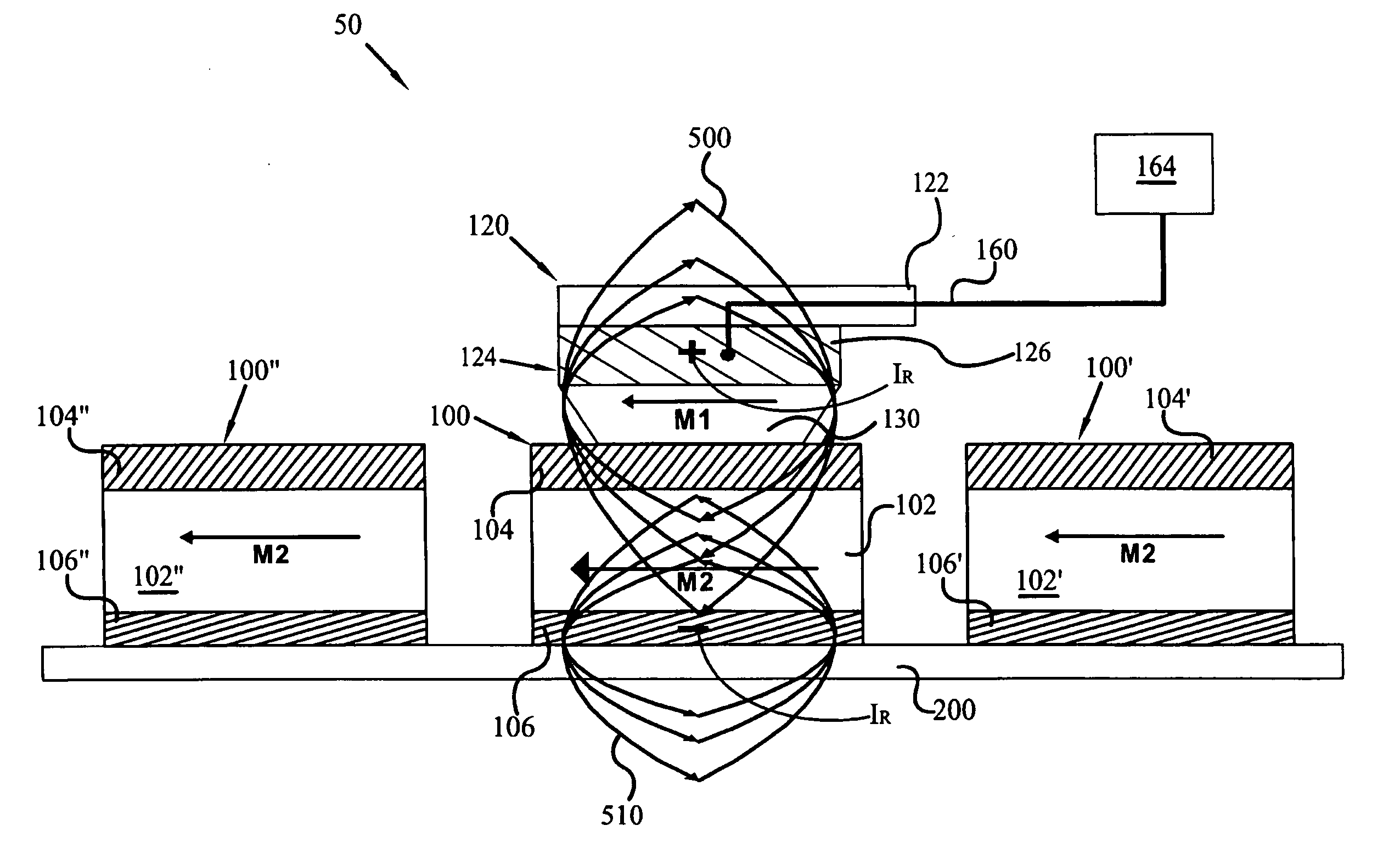
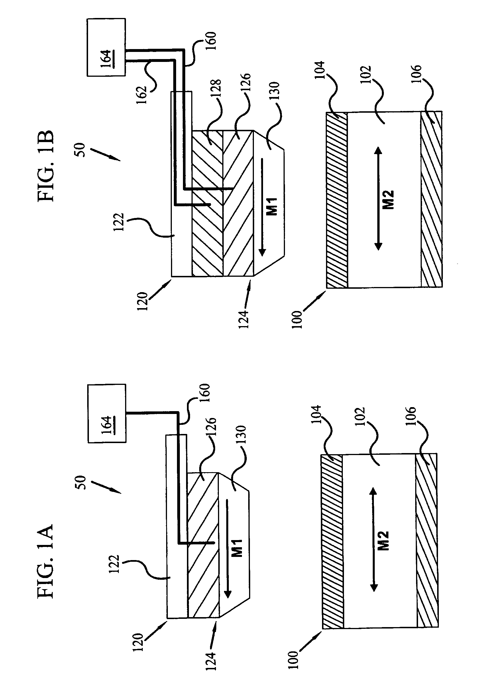
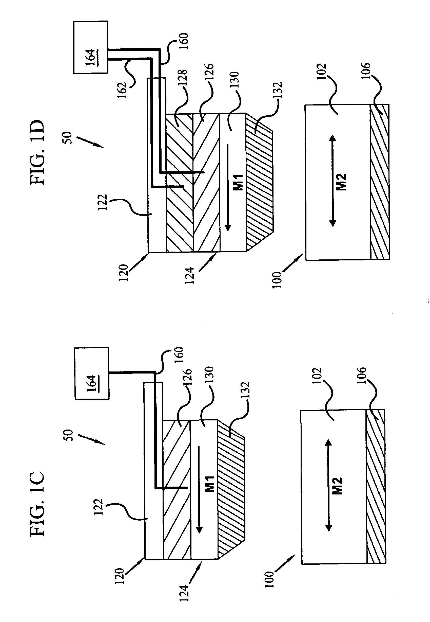
[0033] Referring now to the drawings, and more particularly to FIGS. 1A and 1B, there is shown a portion of a nanotip based magnetic memory with thermally assisted switching 50, having at least one magnetic memory cell 100 and movable probe 120 positioned proximate to the memory cell 100, according to an embodiment of the present invention. In at least one embodiment, the magnetic memory cell 100 may be a divided magnetic tunnel junction memory cell. Specifically, the magnetic memory cell 100 may have a ferromagnetic data layer 102, a intermediate layer 104 and a cond...


PUM

PropertyMeasurementUnit
temperaturesaaaaaaaaaa
thicknessaaaaaaaaaa
magnetizationaaaaaaaaaa

Abstract

This invention provides a probe based magnetic memory storage device. In a particular embodiment, magnetic memory cells are provided in an array. Each cell provides a magnetic data layer and a conductor. At least one movable probe having a tip characterized by a conductor and a soft reference layer is also provided. In addition, an intermediate layer joined to either the movable probe or each memory cell is provided. The movable probe may be placed in contact with a given memory cell, the probe and cell thereby forming a tunnel junction memory cell with the intermediate layer serving as the tunnel junction. The magnetic field provided by the probe conductor may be combined with a field provided by the cell conductor to produce a switching field to alter the orientation of the data layer. The memory cells may include a material wherein the coercivity is decreased upon an increase in temperature. The probe may also include a heat generator. The magnetic field provided by the probe connector will not alter the orientation of an unheated cell, but may alter the orientation of a heated cell.

Description

FIELD OF THE INVENTION [0001] This invention relates generally to ultra-high density thermally assisted magnetic memory devices, and in particular to nanotip probe based magnetic memory arrays. BACKGROUND OF THE INVENTION [0002] Today's computer systems are becoming increasingly sophisticated, permitting users to perform an ever increasing variety of computing tasks at faster and faster rates. The size of the memory and the speed at which it can be accessed bear heavily upon the overall speed of the computer system. [0003] Memory for a computer system is technically any form of electronic, magnetic or optical storage; however it is generally divided up into different categories based in part upon speed and functionality. The two general categories of computer memory are main memory and mass storage. Main memory is generally comprised of fast, expensive volatile random access memory that is connected directly to the processor by a memory buss. [0004] Mass storage devices are typicall...

Claims


Application Information

Patent Timeline
Patent Type & Authority Applications(United States)
IPC IPC(8): H01L27/105G11B5/00G11B5/66G11B5/74G11B9/00G11B11/10G11C11/16H01L21/8246H01L43/08
CPCB82Y10/00G11B5/00G11B5/66G11B5/74G11B5/743G11C11/16G11B9/1418G11B11/10G11B2005/0002G11B2005/0005G11B2005/0021G11B9/1409G11C11/1675
Inventor SHARMA, MANISH
Owner SAMSUNG ELECTRONICS CO LTD
Why Eureka
Try Eureka