

Semiconductor device and method of fabricating the same
a technology of semiconductor devices and semiconductors, applied in semiconductor devices, semiconductor/solid-state device details, electrical apparatus, etc., can solve the problems of reducing processing accuracy in subsequent steps, and achieve the effect of reducing the warping of a base pla
- Summary
- Abstract
- Description
- Claims
- Application Information
AI Technical Summary
Benefits of technology
Problems solved by technology
Method used
Image

Examples
first embodiment
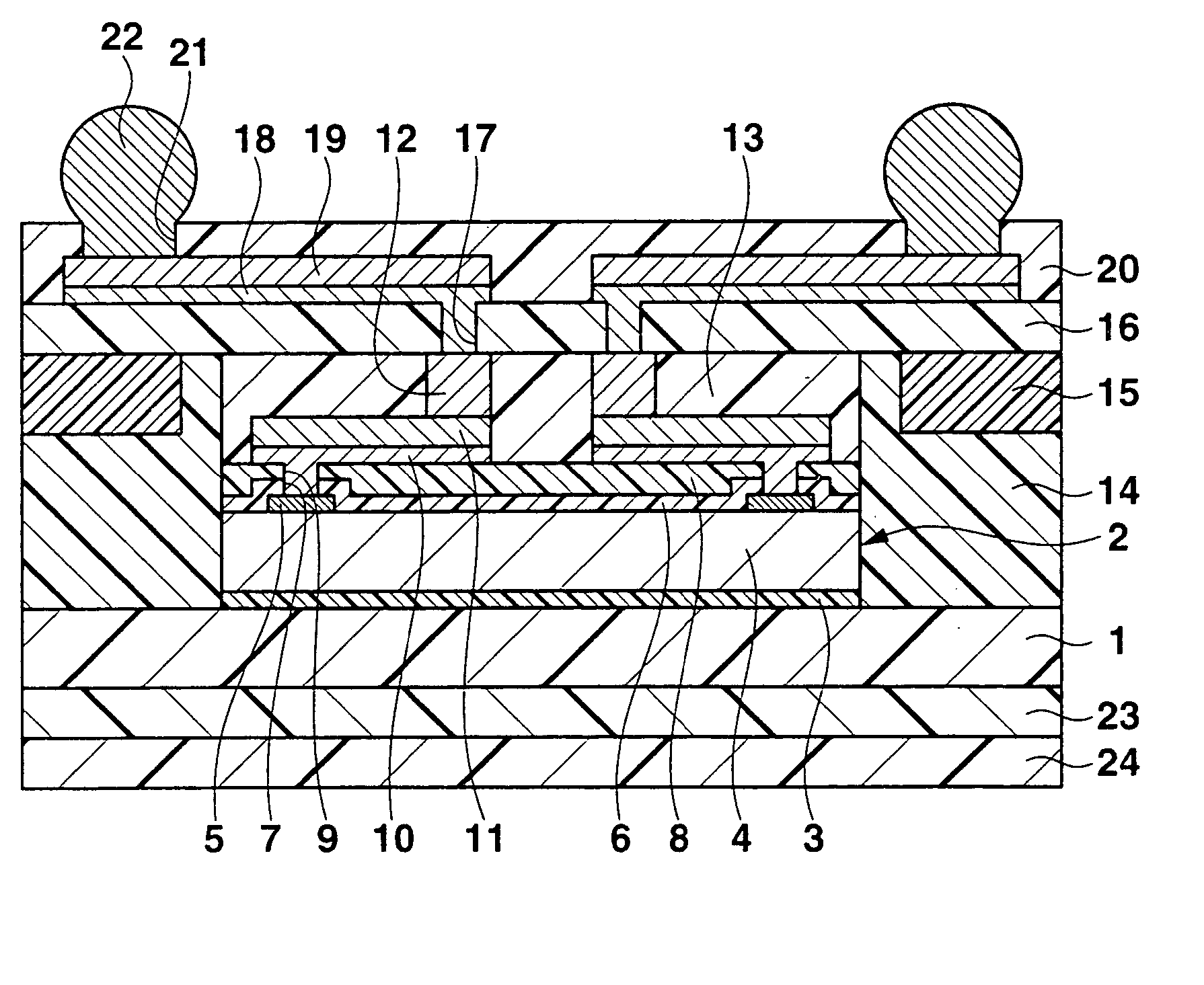
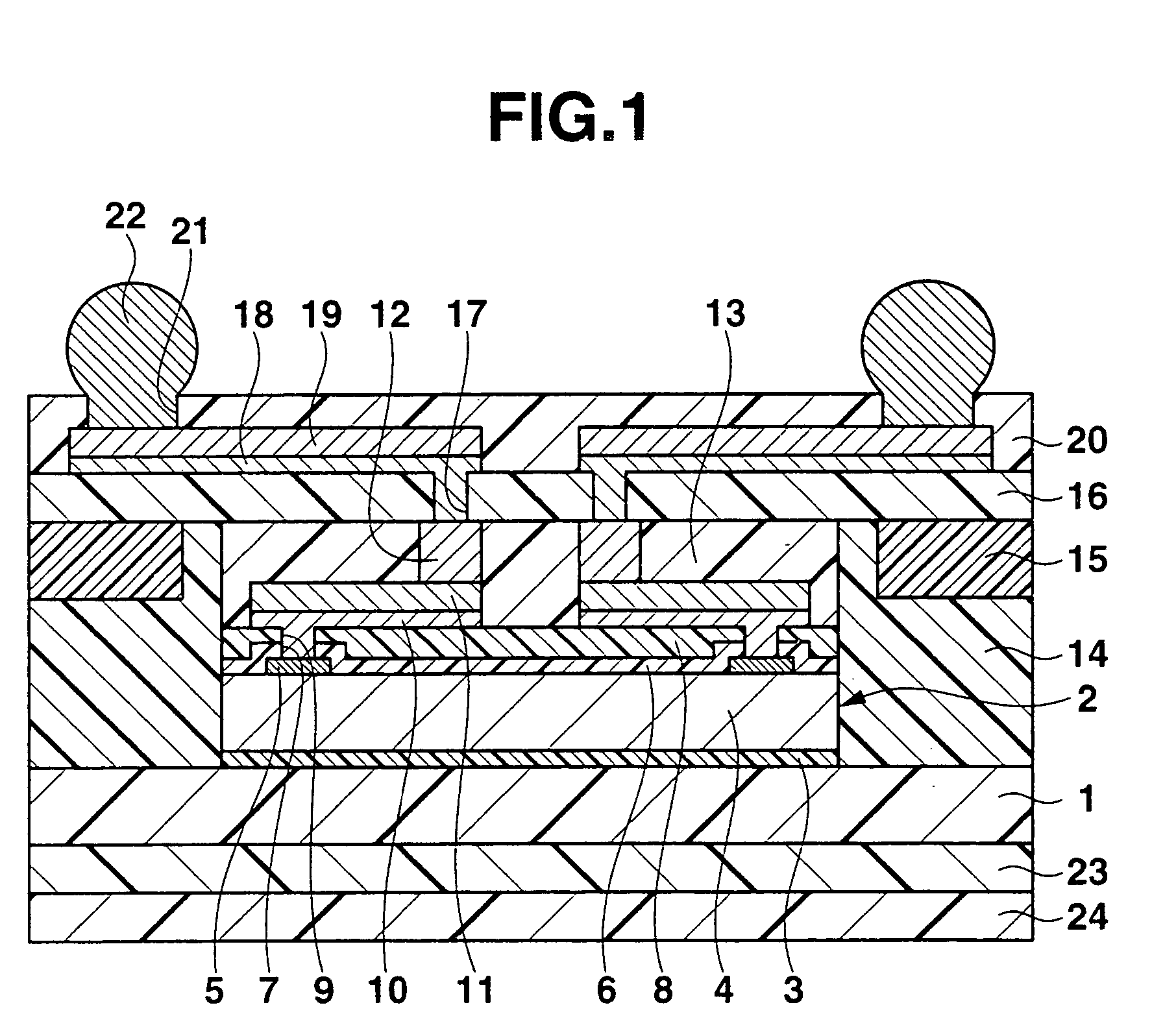
[0043]FIG. 1 is a sectional view of a semiconductor device according to the first embodiment of the present invention. This semiconductor device includes a base plate 1 having a square planar shape. The base plate 1 is made of a material which is generally used as a printed circuit board. Examples of this material are a substrate made of an inorganic material such as glass cloth, glass fibers, or aramid fibers and impregnated with a thermosetting resin such as an epoxy-based resin, polyimide-based resin, or BT (Bismaleimide-Triazine) resin, and a thermosetting resin such as an epoxy-based resin.
[0044] The lower surface of a semiconductor constituent body 2 having a square planar shape and a size smaller to a certain degree than the size of the base plate 1 is adhered to the upper surface of the base plate 1 via an adhesive layer 3 made of a die bonding material. The semiconductor constituent body 2 has interconnections 11, columnar electrodes 12, and an encapsulating film 13 (all o...
second embodiment
[0087]FIG. 18 is a sectional view of an assembly in a predetermined step for explaining the second embodiment of the present invention. In the first embodiment, after the step shown in FIG. 10, the insulating layer 14 and hard sheet 15 are formed as shown in FIG. 11, and the upper insulating film 16 and lower insulating film 23 are formed as shown in FIG. 12.
[0088] By contrast, in the second embodiment of the present invention, after the step shown in FIG. 10, an upper insulating film formation sheet 16a is formed on the upper surface of a hard sheet 15, and a lower insulating film formation sheet 23a is formed on the lower surface of a base plate 1, as shown in FIG. 18. Then, a pair of heating / pressing plates are used to heat and press the resultant structure from above and below, as shown in, e.g., FIG. 12, thereby simultaneously forming an insulating layer 14, hard sheet 15, upper insulating film 16, and lower insulating film 23. In this embodiment, therefore, the number of heat...
third embodiment
[0090]FIG. 19 is a sectional view of an assembly in a predetermined step for explaining the third embodiment of the present invention. In the first embodiment, as shown in FIG. 10, the two lattice-like insulating layer formation sheets 14a and 14b and the lattice-like hard sheet 15 are stacked on the upper surface of the base plate 1 around the semiconductor constituent body 2.
[0091] By contrast, in the third embodiment of the present invention, as shown in FIG. 19, an insulating layer formation layer 14c made of a material containing at least liquid thermosetting resin is formed on the upper surface of a base plate 1 around semiconductor constituent bodies 2 by, e.g., screen printing or spin coating. Then, a lattice-like hard sheet 15 is placed on the upper surface of the insulating layer formation layer 14c.
[0092] Subsequently, an upper insulating film formation sheet 16a is placed on the upper surface of the hard sheet 15, and a lower insulating film formation sheet 23a is plac...
PUM
 Abstract
Description
Claims
Application Information