Mask for laser crystallization and crystallization method using the same

a laser crystallization and mask technology, applied in the field of crystallization methods of silicon thin films, can solve the problems of masks being misaligned over the alignment margin, masks may be misaligned, and the top surface of silicon films is apt to oxidize,

Active Publication Date: 2005-06-30
LG DISPLAY CO LTD
View PDF1 Cites 53 Cited by
  • Summary
  • Abstract
  • Description
  • Claims
  • Application Information

AI Technical Summary

Problems solved by technology

However, since the surface temperature of the irradiated amorphous silicon film reaches about 1400° C., the top surface of the silicon film is apt to oxidize.
However, when the mask for laser crystallization is changed, the mask may be misaligned over the alignment margin.
Specifically, the misalignment o

Method used


Image

  • Mask for laser crystallization and crystallization method using the same
  • Mask for laser crystallization and crystallization method using the same
  • Mask for laser crystallization and crystallization method using the same

Examples


first embodiment

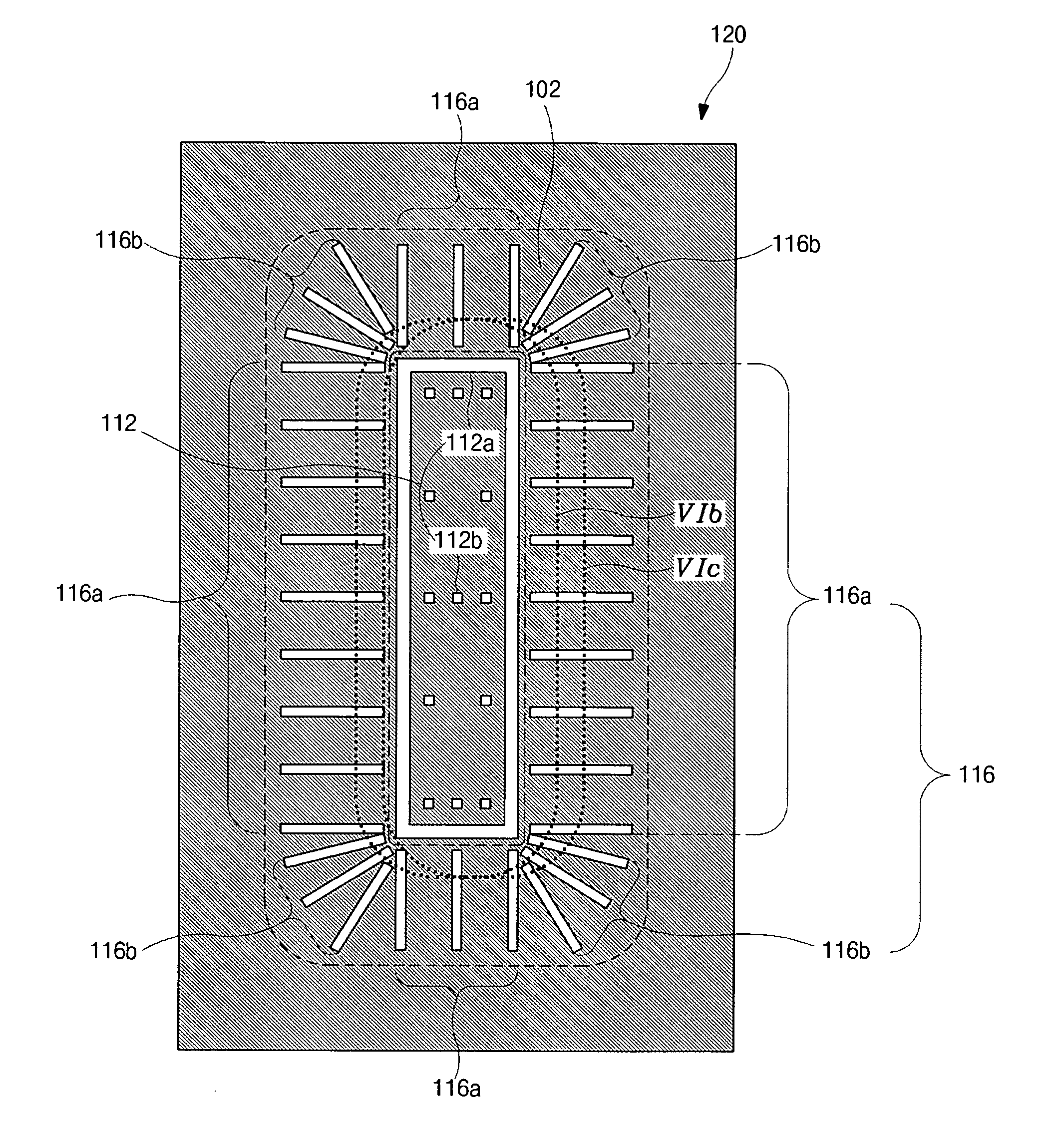
[0037]FIG. 5 is a schematic plane view showing a mask for laser crystallization according to the present invention and FIG. 6 is a magnified view of a portion “VIa” of FIG. 5. In FIGS. 5 and 6, a pattern corresponds to a transmissive portion through which a laser beam passes and a shaded region surrounding the pattern corresponds to a shielding portion 102 where the laser beam is blocked.

[0038] In FIG. 5, a mask 100 for laser crystallization includes a crystallization pattern 110 used for a laser crystallization process and an alignment pattern 120 adjacent to the crystallization pattern 110. The alignment pattern 120 includes a first pattern group 112 having a corresponding size to the crystallization pattern 110 and a second pattern group 116 surrounding the first pattern group 112. The second pattern group 116 has a plurality of radial bars.

[0039] In FIG. 6, the alignment pattern 120 includes a first pattern group 112 and a second pattern group 116. The first pattern group 112 c...

fourth embodiment

[0049]FIG. 8 is a schematic cross-sectional view showing a mask for crystallization according to the present invention.

[0050] In FIG. 8, a mask 250 for laser crystallization includes a crystallization pattern 252 and an alignment pattern 254. For example, the crystallization pattern 252 may include first, second and third sub-crystallization patterns 252a, 252b and 252c different from one another. The alignment pattern 254 includes a first pattern group 254a having a size corresponding to one of the first, second and third sub-crystallization pattern 252a, 252b and 252c and a second pattern group 254b surrounding the first pattern group 254a. The second pattern group 254b has a plurality of radial bars.

[0051] Before crystallizing an amorphous silicon layer using a laser beam, the laser beam is aligned with the mask for laser crystallization by using the alignment pattern 254, i.e., measuring a length of polycrystalline silicon patterns corresponding to the radial bars of the second...


PUM

PropertyMeasurementUnit
Sizeaaaaaaaaaa
Distanceaaaaaaaaaa
Energy densityaaaaaaaaaa

Abstract

A mask for laser crystallization includes a transmissive portion defining a crystallization pattern and an alignment pattern. The alignment pattern includes a first pattern group having a size corresponding to the crystallization pattern and a second pattern group having a plurality of radial bars surrounding the first pattern group. A shielding portion surrounds the transmissive portion.

Description

[0001] This application claims the benefit of Korean Patent Application No. 2003-97879, filed on Dec. 26, 2003, which is hereby incorporated by reference. BACKGROUND [0002] 1. Field [0003] The present application relates to a crystallization method of a silicon thin film, and more particularly, to a mask for laser crystallization and a crystallization method using the mask. [0004] 2. Discussion of the Related Art [0005] Flat panel display (FPD) devices having high portability and low power consumption have been the subject of recent research and development. Among various types of FPD devices, liquid crystal display (LCD) devices are commonly used as monitors for notebook and desktop computers because of their ability to display high-resolution images, wide ranges of different colors, and moving images. [0006] In general, an LCD device includes a color filter substrate and an array substrate separated from each other by a liquid crystal layer. The color filter substrate and the arra...

Claims


Application Information

Patent Timeline
IPC IPC(8): G02F1/13B23K26/06G03F9/00H01L21/00H01L21/20H01L21/77H01L21/84
CPCB23K26/0656H01L27/1285H01L21/2026G03F9/7076B23K26/066H01L21/02532H01L21/0268G02F1/13
Inventor YOU, JAESUNG
Owner LG DISPLAY CO LTD
Why Eureka
Try Eureka