Securities, chip mounting product, and manufacturing method thereof

a technology of security and mounting products, applied in the field of thin film integrated circuits, can solve the problems of affecting the reliability of ic cards, ic chips formed over silicon wafers have a problem of low impact resistance, so as to reduce costs, reduce costs, and increase productivity

Inactive Publication Date: 2005-07-07
SEMICON ENERGY LAB CO LTD
View PDF79 Cites 61 Cited by
  • Summary
  • Abstract
  • Description
  • Claims
  • Application Information

AI Technical Summary

Benefits of technology

[0030] As being formed on an insulating surface, the chip of the invention can be reduced in cost as compared with a conventional chip formed over a silicon wafer. In particular, a chip formed over a circular silicon wafer has a limit in the size and shape of a mother substrate. Meanwhile, the chip of the invention does not have a limit in the size and shape of a mother substrate since an insulating substrate such as a glass substrate is employed. Therefore, the productivity is increased and mass production can be achieved, resulting in further reduction in cost. In the integrated circuit with extremely low unit price such as a chip, the cost reduction leads to great profits.
[0031] In addition, the thin film integrated circuit can be formed over a flexible substrate formed of a synthetic resin, thus it is expected that the impact resistance of the chip is increased.
[0032] Further, the thin film integrated circuit of the invention is drastically reduced in thickness as compared with a conventional integrated circuit formed over a silicon wafer, and can transmit light. Accordingly, the thin film integrated circuit of the invention can be attached to products while maintaining an attractive design.
[0033] According to such a thin film integrated circuit of the invention, the exchange or the management of data can be performed more simply and in a shorter time, and various data exchange can be achieved as compared with other data exchange means such as bar code.

Problems solved by technology

However, an IC chip formed over a silicon wafer is more expensive than a magnetic card.
The IC chip formed over a silicon wafer has a problem of low impact resistance since it is made thin to be used as a card.
In particular, an increased area of the IC chip adversely affects the reliability of an IC card.
As a result, the design of the products and goods becomes less attractive.

Method used


Image

  • Securities, chip mounting product, and manufacturing method thereof
  • Securities, chip mounting product, and manufacturing method thereof
  • Securities, chip mounting product, and manufacturing method thereof

Examples


embodiment mode 1

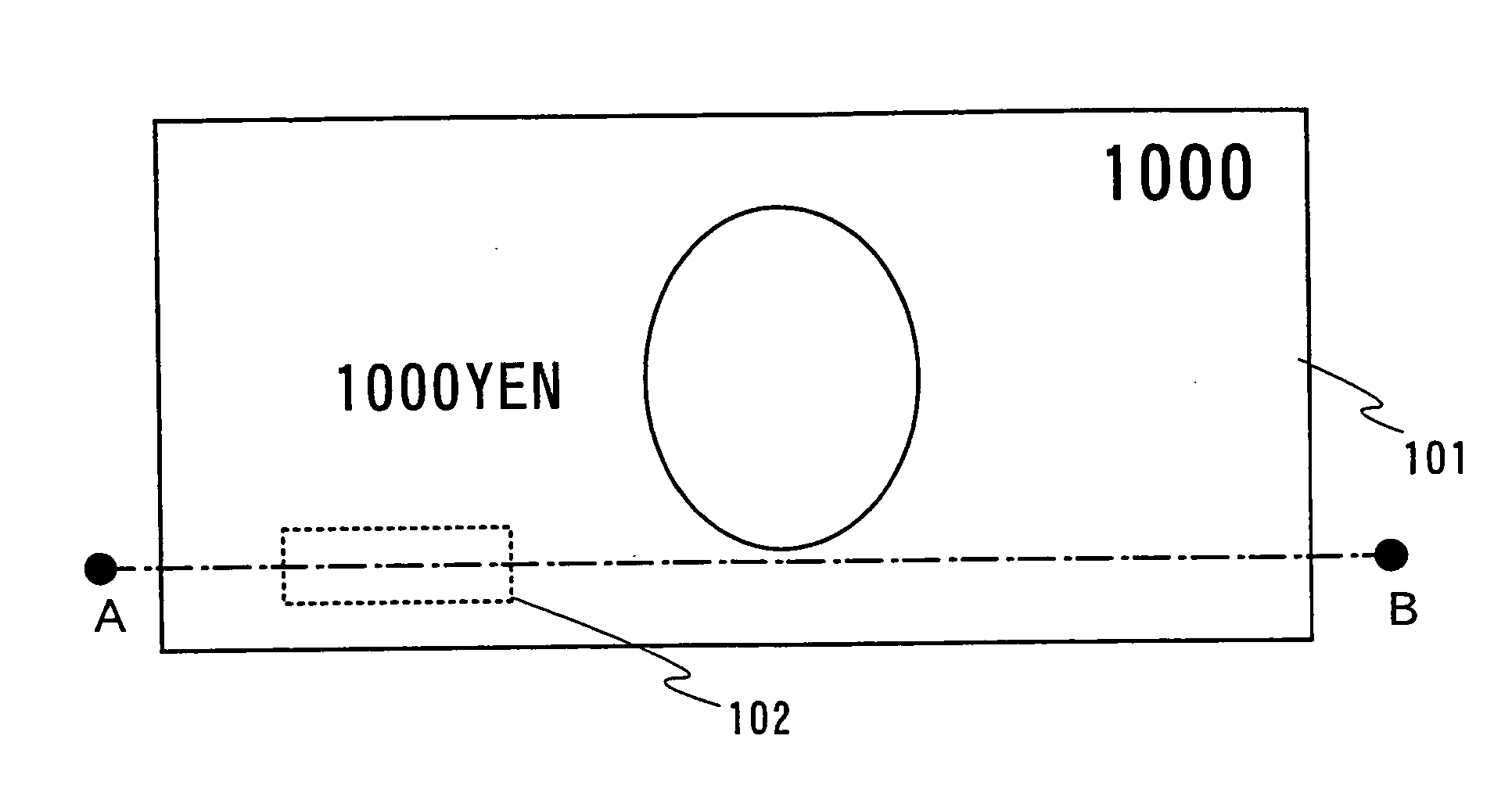
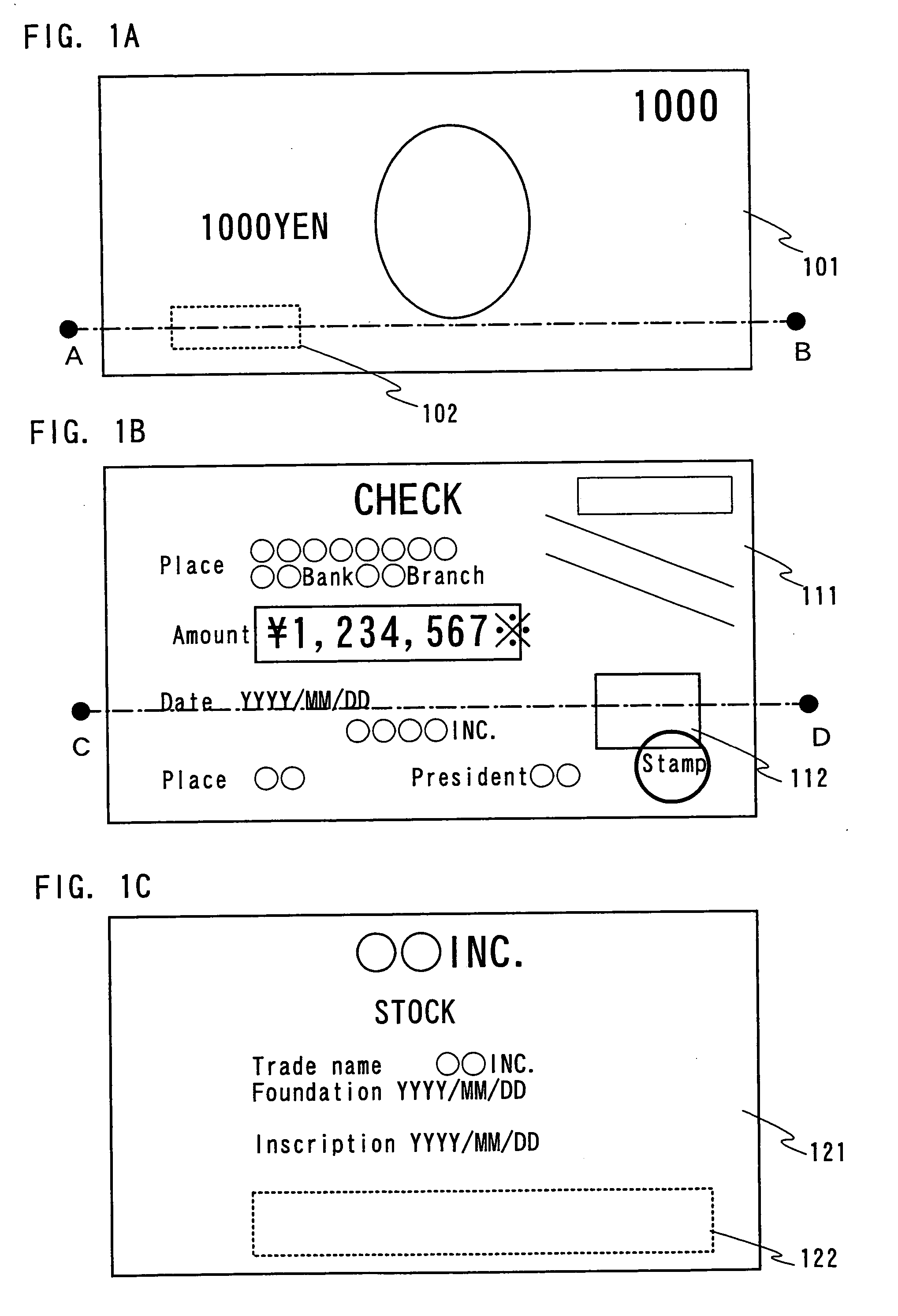
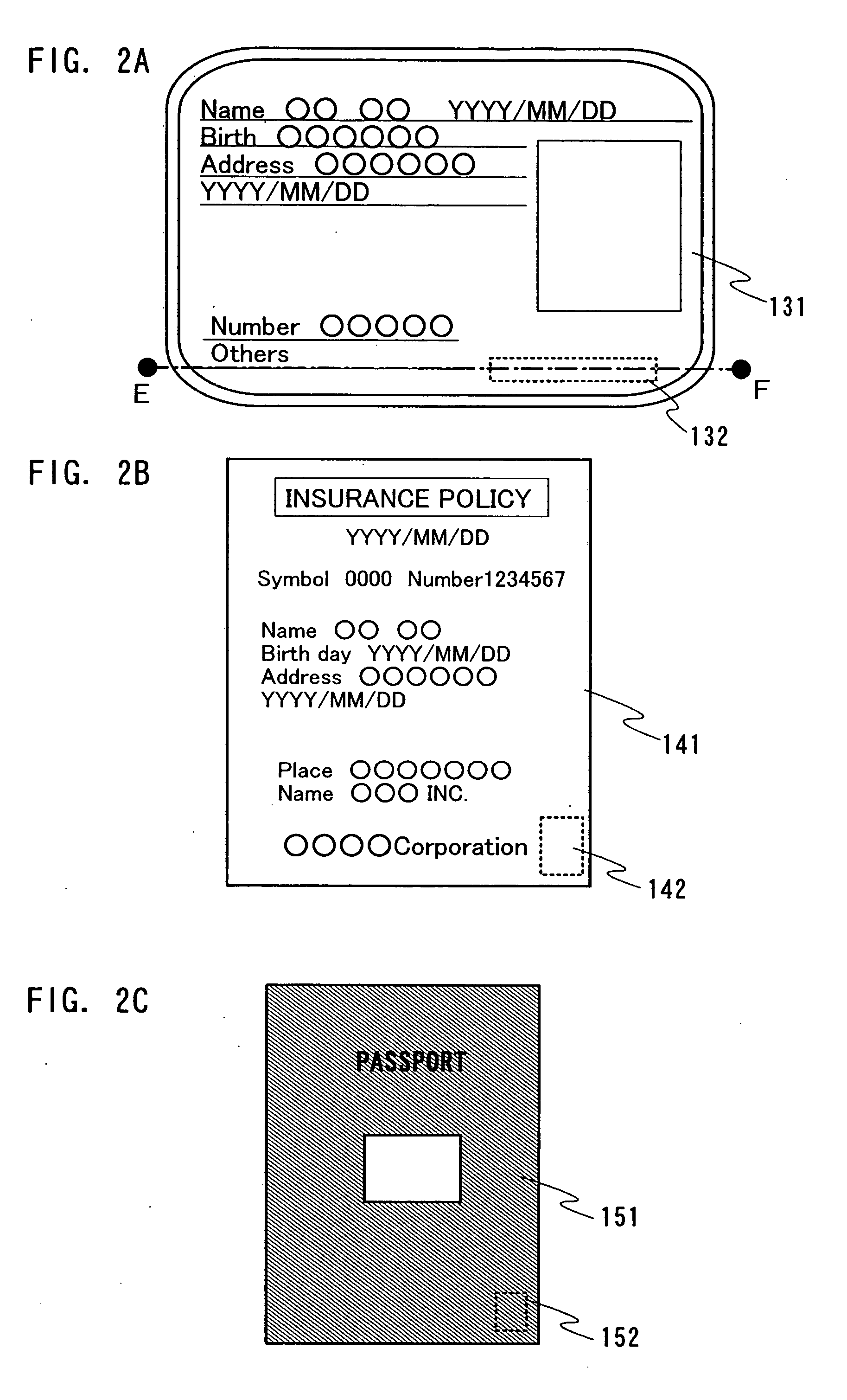
[0061] Described in this embodiment mode are products each mounting an ID chip. The position, the size and shape, and the number of mounted ID chips are not limited to the ones shown in this embodiment mode.

[0062] When a memory such as a ROM to which data cannot be rewritten is formed in a thin film integrated circuit included in an ID chip, it is possible to prevent forgery of securities such as bills and checks, and certificates such as a family register, a resident card, a traveler's check, and a passport. In addition, when a wireless tag of the invention is used for foods whose commercial value depends crucially on a production area, a producer and the like, forgery of production area, producer and the like can be prevented at low cost.

[0063] Various products mounting an ID chip are shown below.

[0064]FIG. 1A shows a bill 101 mounting an ID chip. Although an ID chip 102 is mounted inside the bill 101 in FIG. 1A, it may be exposed on a surface thereof.

[0065] The bill may be pr...

embodiment mode 2

[0116] As set forth above, a thin film integrated circuit and an antenna are required for a contactless ID chip. Various arrangements are available for the antenna, and a connecting terminal connected to the thin film integrated circuit may be provided at the end of the antenna. Described in this embodiment mode are the size and shape, manufacturing method and mounting method of the antenna that is incorporated in the ID chip.

[0117] First, the size and shape of an antenna are explained.

[0118] For example, an antenna 515 is formed over a substrate 516 for mounting the antenna (hereinafter referred to as an antenna substrate) so as to be twisted, and a connecting terminal 517 is provided at the end of the antenna 515 as shown in FIG. 7A. The connecting terminal 517 may be disposed anywhere, and the arrangement thereof can be determined depending on a connecting terminal of a thin film integrated circuit.

[0119] An antenna 515 may wind in a rectangular shape, and a connecting termina...

embodiment mode 3

[0153] Described in this embodiment mode is the case of mounting an ID chip on a curved surface of a product in particular.

[0154] In FIG. 10A, a plurality of thin film integrated circuits 501 are formed over the large substrate 500 having an insulating surface. Cost reduction of the ID chip can be achieved by forming a plurality of thin film integrated circuits over a large substrate, namely by a multiple pattern technology.

[0155] A semiconductor film of the thin film integrated circuit may be any one of an amorphous semiconductor, a semi-amorphous semiconductor (referred to as an SAS) having an intermediate structure between amorphous and crystalline structures, and a crystalline semiconductor. The SAS includes a microcrystalline semiconductor having crystal grains of 0.5 to 20 nm in an amorphous semiconductor. In particular, a microcrystalline state having crystal grains of 0.5 to 20 nm is called a microcrystal (μc).

[0156] In this embodiment mode, an amorphous semiconductor fil...


PUM


Abstract

The invention provides an ID chip with reduced cost, increased impact resistance and attractive design, as well as products and the like mounting the ID chip and a manufacturing method thereof. In view of the foregoing, an integrated circuit having a semiconductor film with a thickness of 0.2 μm or less is mounted on securities including bills, belongings, containers of food and drink, and the like (hereinafter referred to as products and the like). The ID chip of the invention can be reduced in cost and increased in impact resistance as compared with a chip formed over a silicon wafer while maintaining an attractive design.

Description

BACKGROUND OF THE INVENTION [0001] 1. Field of the Invention The present invention relates to a thin film integrated circuit formed on an insulating surface and a chip incorporating the thin film integrated circuit. In particular, the invention relates to securities mounting the chip, other products mounting the chip, and a manufacturing method thereof. [0002] 2. Description of the Related Art In recent years, there has been an increased need for an IC card or an IC tag capable of wireless data communication in all fields that require automatic identification, such as securities and goods management. Such an IC card or an IC tag is required to be small and inexpensive in view of the increased impact resistance and disposable application respectively, to have an affinity for paper particularly in view of the management of securities, and to have a high capacity memory in accordance with the increased amount of data. Thus, in order to meet such requirements, the development of an IC c...

Claims


Application Information

Patent Timeline
Patent Type & Authority Applications(United States)
IPC IPC(8): G06K19/06G06K19/077G07D7/00H01L23/02H01L23/498
CPCG06K19/07749G06K19/07758G06K19/07767G07D7/0093H01L2924/0002H01L23/49855H01L2924/00G07D7/01
Inventor YAMAZAKI, SHUNPEIKATO, KIYOSHI
Owner SEMICON ENERGY LAB CO LTD
Why Eureka
Try Eureka