Seal ring for integrated circuits

a technology of integrated circuits and seal rings, which is applied in the direction of semiconductor devices, semiconductor/solid-state device details, electrical apparatus, etc., can solve the problems of reducing the ability of the semiconductor to communicate electrical signals, more specifically noise, and diminishing so as to reduce the ability of the semiconductor and diminish the protective benefits of the seal ring

Inactive Publication Date: 2005-07-07
AVAGO TECH INT SALES PTE LTD
View PDF15 Cites 15 Cited by
  • Summary
  • Abstract
  • Description
  • Claims
  • Application Information

AI Technical Summary

Benefits of technology

[0010] Allowing the substrate to electrically contact the seal ring only at a minor portion of the seal ring ensures that the short circuit between the seal ring and the substrate is limited to a small portion of the semiconductor die. Thus, the only low resistance electrical path between the substrate and the seal ring is confined to the small portion of the seal ring in electrical contact with the gap in the elongate region. With only one low resistance electrical path between the seal ring and the substrate, the seal ring no longer behaves as a conductive ring interconnecting all areas of the semiconductor die. The direct contact between the seal ring and the substrate at the gap is sufficient, however, to prevent the seal structure from accumulating charge while being manufactured. The location of the minor portion of the seal ring that contacts the substrate can be adjusted and optimized according to the specific circuit requirements.
[0012] As mentioned above, the substrate and the well region of the preferred embodiment are formed having opposite conductivity types. The present invention allows for the substrate to have either a p-type or n-type conductivity, and the elongate region may be a well having either an n-type or p-type conductivity, respectively. Forming a well region with a conductivity opposite that of the substrate of the semiconductor die, and bringing the majority of the seal ring into physical contact only with the well region, reduces the ability of the semiconductor to communicate electrical signals, more specifically noise, through the seal ring to noise sensitive areas of the semiconductor die, without diminishing the protective benefits of the seal ring during manufacture of the die and during use of the semiconductor.

Problems solved by technology

Forming a well region with a conductivity opposite that of the substrate of the semiconductor die, and bringing the majority of the seal ring into physical contact only with the well region, reduces the ability of the semiconductor to communicate electrical signals, more specifically noise, through the seal ring to noise sensitive areas of the semiconductor die, without diminishing the protective benefits of the seal ring during manufacture of the die and during use of the semiconductor.

Method used


Image

  • Seal ring for integrated circuits
  • Seal ring for integrated circuits
  • Seal ring for integrated circuits

Examples


Embodiment Construction

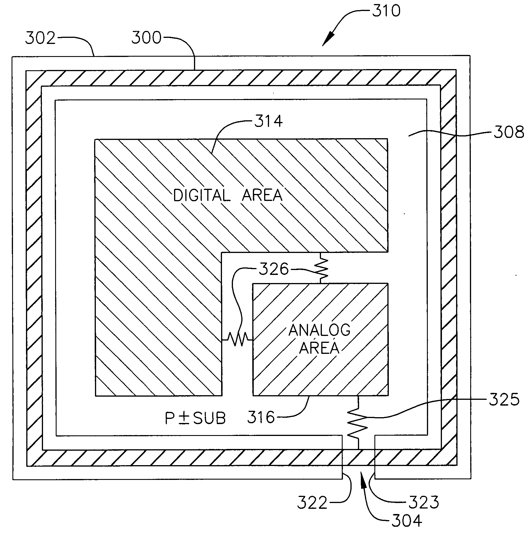
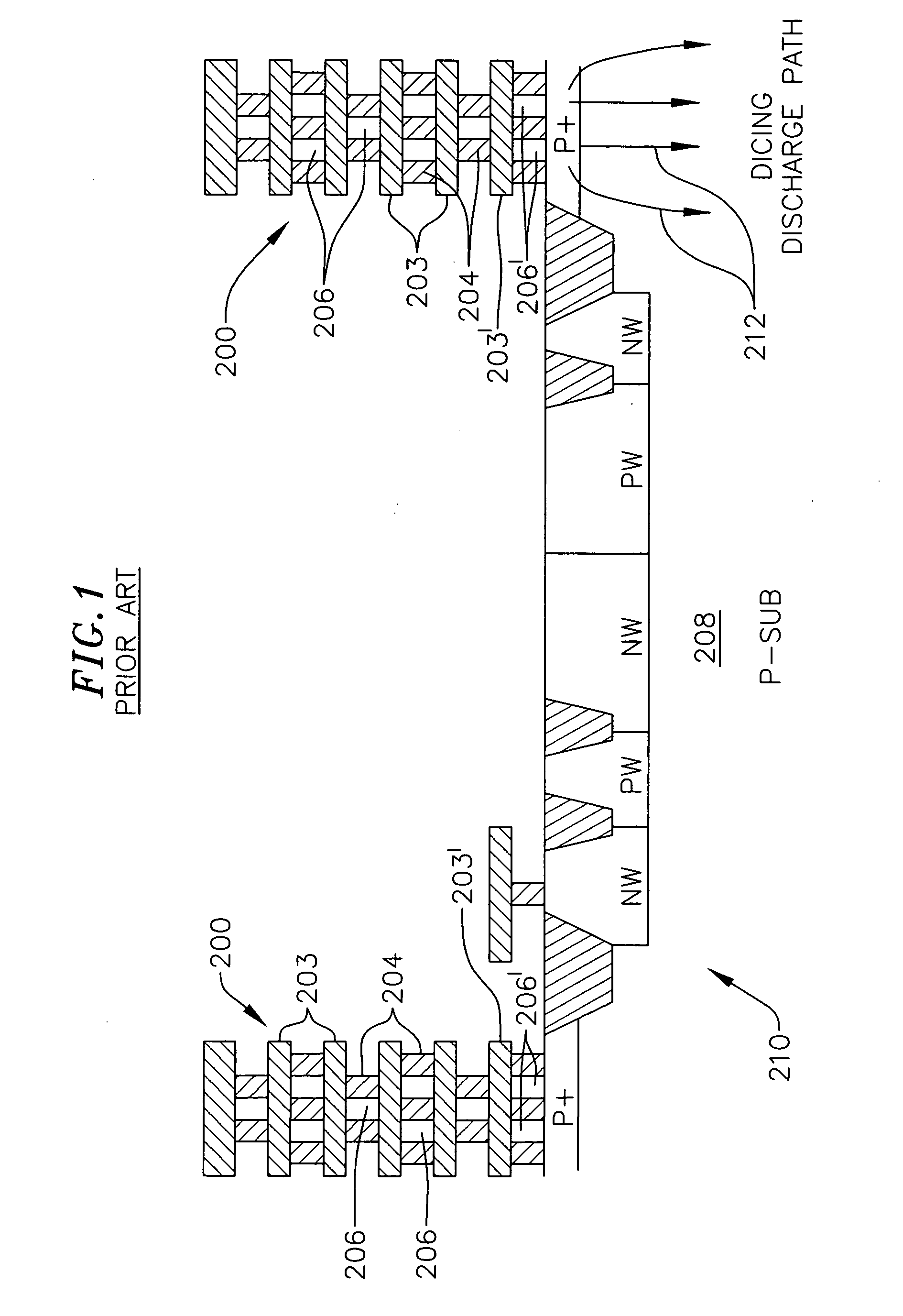
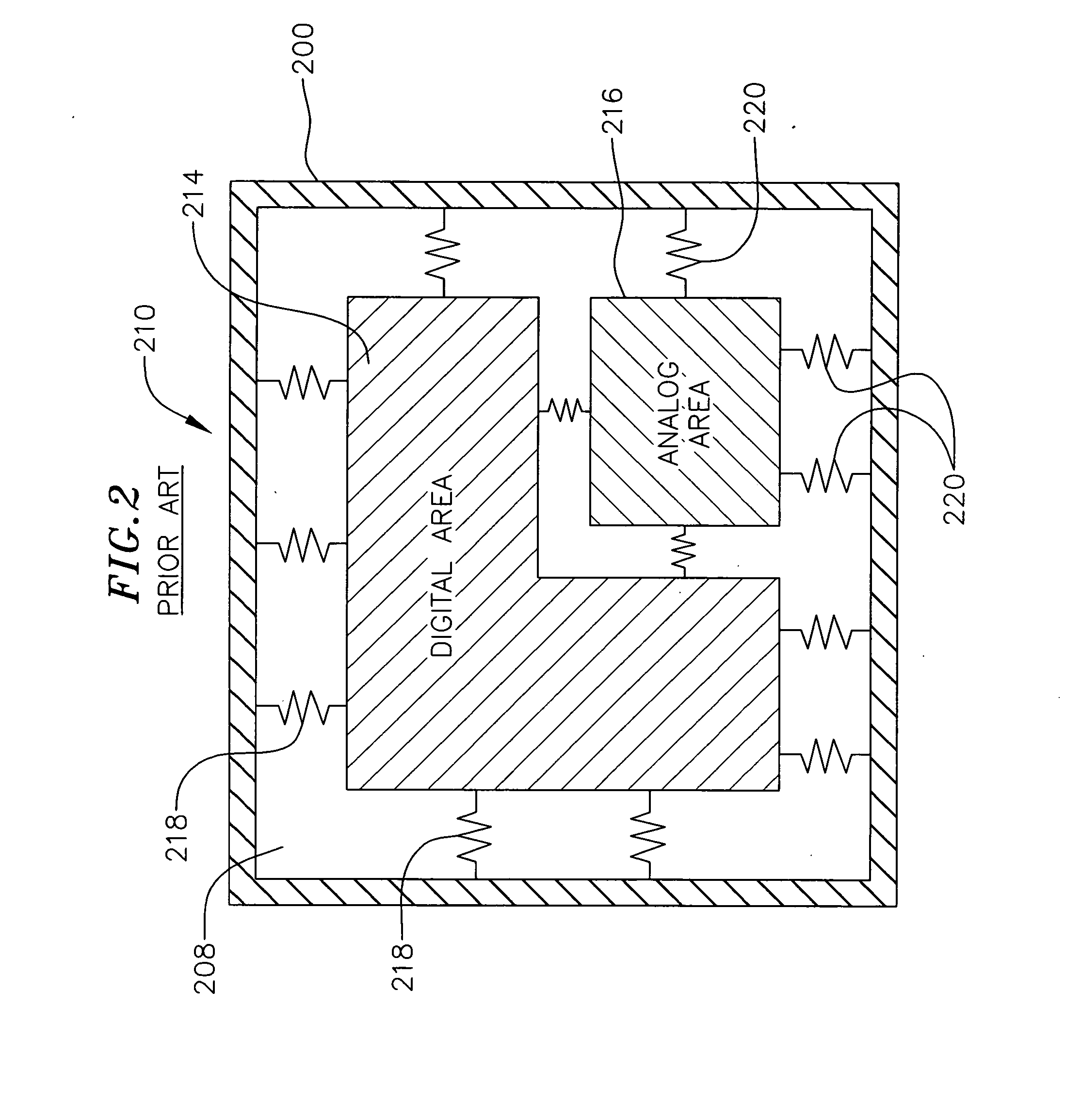
[0018] A prior art semiconductor die 210 employing a seal ring structure 200 formed on a substrate 208 is illustrated by way of reference to FIG. 1. Seal ring 200 is composed of alternating conductive metal layers 203 and insulating layers 204. Each insulating layer 204 contains one or more vias 206 extending through the insulating layer and providing a conductive path between various metal layers 203. The lowest conductive metal layer 203′ of seal 200 contacts substrate 208 through vias 206′ to provide a relatively low resistance conductive path between the seal ring and the substrate of semiconductor die 210. Substrate 208 is typically silicon, but may consist of other materials.

[0019]FIG. 1 shows substrate 208 as having a p-type conductivity. Alternatively, substrate 208 could have an n-type conductivity. In either event, substrate 208 is rendered partially conducting. Dicing discharging paths 212 are created in substrate 208 at the point at which the lowest conductive metal lay...


PUM


Abstract

The present invention is directed to a seal structure and a method for forming a seal structure for a semiconductor die. An elongate region which is electrically isolated from the remainder of the substrate, such as a well region of a conductivity type opposite that of the substrate, extends around the major portion of the periphery of the substrate. A gap is left between the two ends of the elongate region along the minor portion of the periphery of the substrate not covered by the elongate region. A conductive seal ring is formed around the periphery of the substrate at the elongate region and spans the gap between the ends of the elongate region. The substrate of the semiconductor die is only brought into electrical contact with the seal ring at the gap between the ends of the elongate region.

Description

CROSS-REFERENCES TO RELATED APPLICATIONS [0001] This application is a continuation of U.S. patent application Ser. No. 09 / 650,275 filed Aug. 29, 2000 which claims priority from U.S. Provisional Patent Application Ser. No. 60 / 191,341 filed Mar. 22, 2000, the disclosures of each of which are incorporated herein by reference.BACKGROUND OF THE INVENTION [0002] 1. Field of the Invention [0003] The present invention relates generally to the manufacture of integrated circuits and more particularly, to a seal structure for a semiconductor die that improves substrate isolation. [0004] 2. Description of the Prior Art [0005] Most semiconductor integrated circuit manufacturers require a seal ring at the periphery of the semiconductor die. The seal ring circumscribes the periphery of the semiconductor die and is in contact with the die. The seal ring surrounds the bonding pads, which are typically disposed along the outer edges of the die. The seal ring creates a barrier to penetration of moistu...

Claims


Application Information

Patent Timeline
Patent Type & Authority Applications(United States)
IPC IPC(8): H01L21/82H01L23/00H01L23/58H01L29/00H01L29/73H01L29/76
CPCH01L23/562H01L23/585H01L2924/0002H01L2924/00
Inventor GUTIERREZ, GERMAN
Owner AVAGO TECH INT SALES PTE LTD
Why Eureka
Try Eureka