Flip chip package structure and chip structure thereof

Inactive Publication Date: 2005-07-07
ADVANCED SEMICON ENG INC
View PDF7 Cites 4 Cited by
  • Summary
  • Abstract
  • Description
  • Claims
  • Application Information

AI Technical Summary

Benefits of technology

[0008] The present invention provides a flip chip package structure and a chip structure, which enhances connection bet

Problems solved by technology

However, as the operation speed of the chip becomes faster and the operation temperature becomes higher, the thermal stress resulting from the mismatch of coefficients of thermal expansion (CTE) between the chip and the substrate becomes larger.
During thermal cycles, the large thermal stress may cause bumps break or peel from th

Method used


Image

  • Flip chip package structure and chip structure thereof
  • Flip chip package structure and chip structure thereof
  • Flip chip package structure and chip structure thereof

Examples


Embodiment Construction

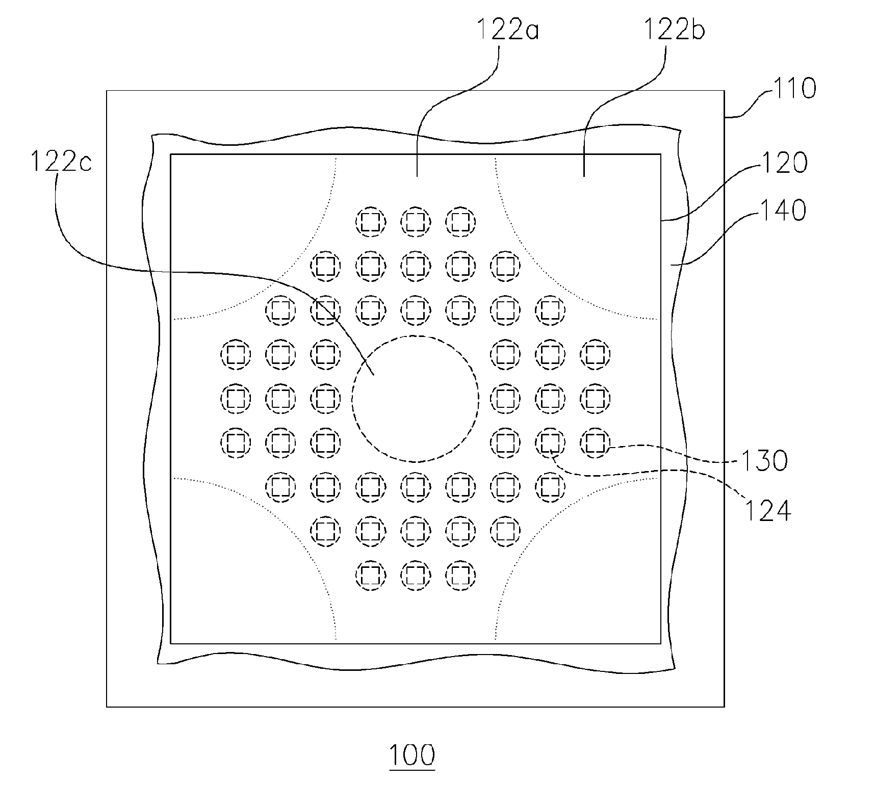
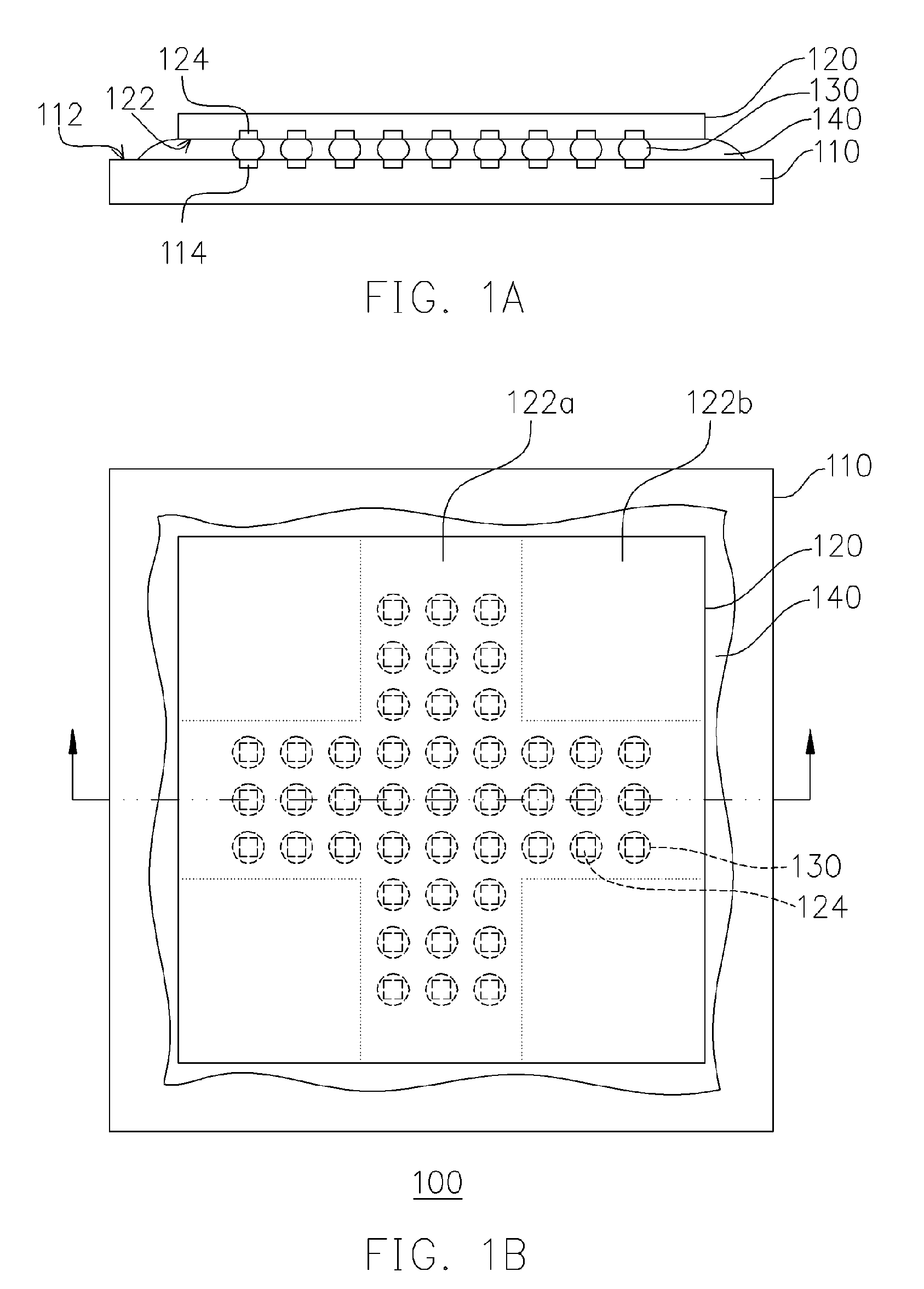
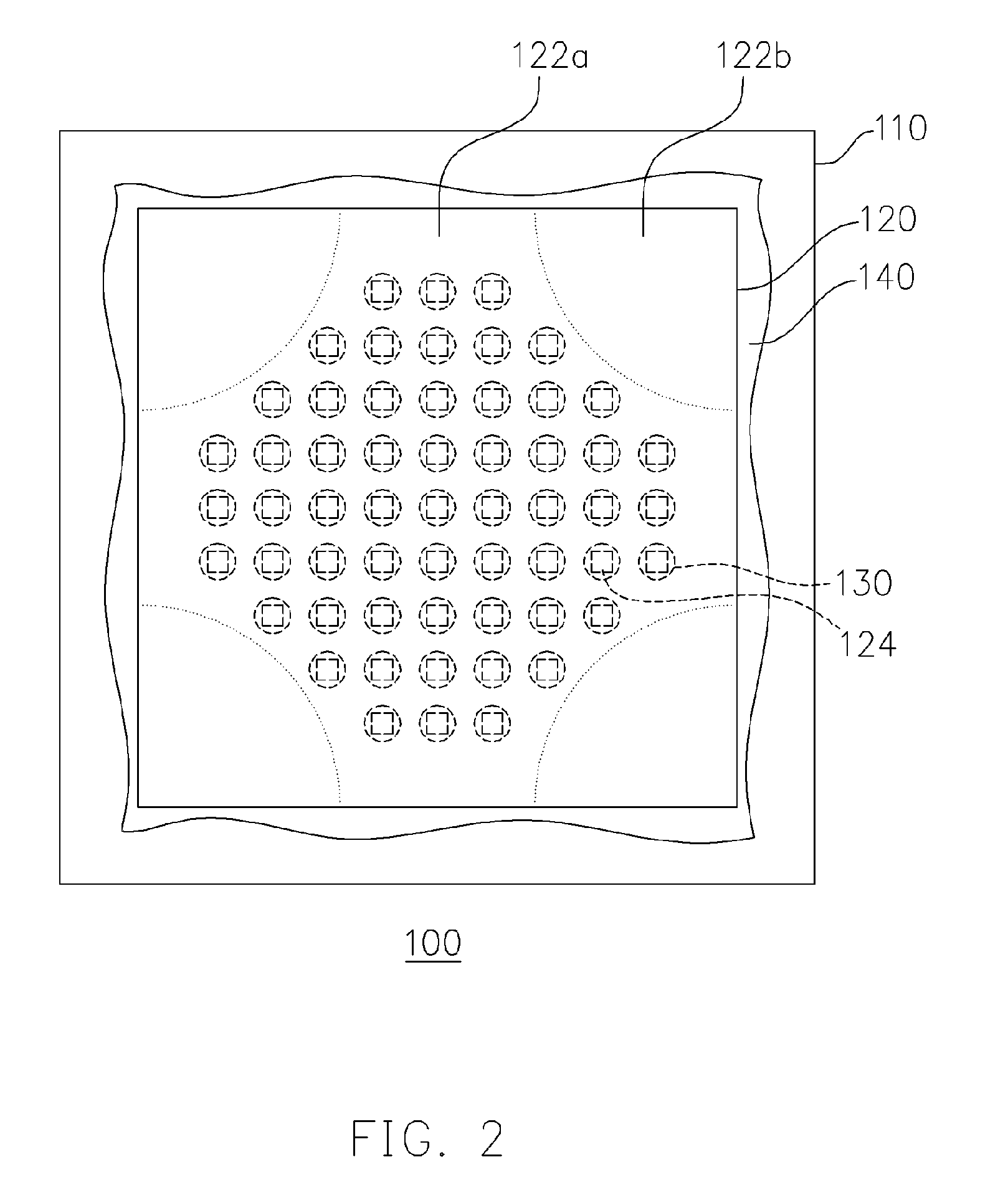
[0022]FIG. 1A is a cross-sectional display view illustrating a flip chip package structure according to the first preferred embodiment of this invention, while FIG. 1B is a top display view illustrating a flip chip package structure according to the first preferred embodiment of this invention. Referring to FIG. 1A, the flip chip package structure 100 includes a chip 120 disposed on a substrate 110. A carrying surface 112 of the substrate 110 are electrically connected to an active surface 122 of the chip 120 through bumps 130. An underfill 140 is filled between the chip 120 and the substrate 110 and wraps the bumps 130. A plurality of contacts 114 is disposed on the carrying surface 112 of the substrate 110.

[0023] Referring to FIG. 1B, a rectangular region at each corner of the active surface 122 is arranged as a non-bumping region 122b, while the other regions of the active surface 122 are arranged as a bumping region 122a. A plurality of bonding pads 124 are disposed on the acti...


PUM


Abstract

The present invention provides a flip chip package structure comprising a substrate, a chip and a plurality ofbumps. A plurality of contacts is disposed on the carrying surface and the chip is disposed on the carrying surface of the substrate. The chip includes an active surface and a plurality of bonding pads. The active surface of the chip comprises a bumping region and a plurality of non-bumping regions at corners of the chip, while the bonding pads are disposed within the bumping region of the active surface of the chip. The bumps, respectively disposed on the bonding pads, electrically and mechanically connect the contacts and the bonding pads.

Description

CROSS-REFERENCE TO RELATED APPLICATION [0001] This application claims the priority benefit of Taiwan application Serial no. 92131927, filed on Nov. 14, 2003. BACKGROUND OF THE INVENTION [0002] 1. Field of Invention [0003] The present invention relates to a package structure. More particularly, the present invention relates to a flip chip package structure and a chip structure thereof, with better connection between the chip and the substrate. [0004] 2. Description of Related Art [0005] In the semiconductor industry, integrated circuits (ICs) manufacture can be categorized as three major stages: fabrication of the wafers, fabrication of the ICs and packaging of the ICs. Through wafer preparation, circuitry design, mask fabrication and wafer dicing, the bare dies are obtained. Each die has bonding pads for outwardly electrical connections. By using the molding materials to achieve the encapsulation of the die, the die is protected from the influences of moisture, heat and noises. The ...

Claims


Application Information

Patent Timeline
IPC IPC(8): H01L21/44H01L21/60H01L23/00H01L23/28H01L23/50
CPCH01L23/50H01L23/562H01L2924/01033H01L2224/81801H01L2924/14H01L24/81H01L2924/351H01L2924/00
Inventor CHEN, YU-WENCHIU, CHI-HAOKAO, CHUNG-YAOKAO, MING-CHIEH
Owner ADVANCED SEMICON ENG INC
Why Eureka
Try Eureka