Surface-emitting type semiconductor laser and method of manufacturing the same
- Summary
- Abstract
- Description
- Claims
- Application Information
AI Technical Summary
Benefits of technology
Problems solved by technology
Method used
Image
Examples
first exemplary embodiment
1. First Exemplary Embodiment
1-1. Device Structure
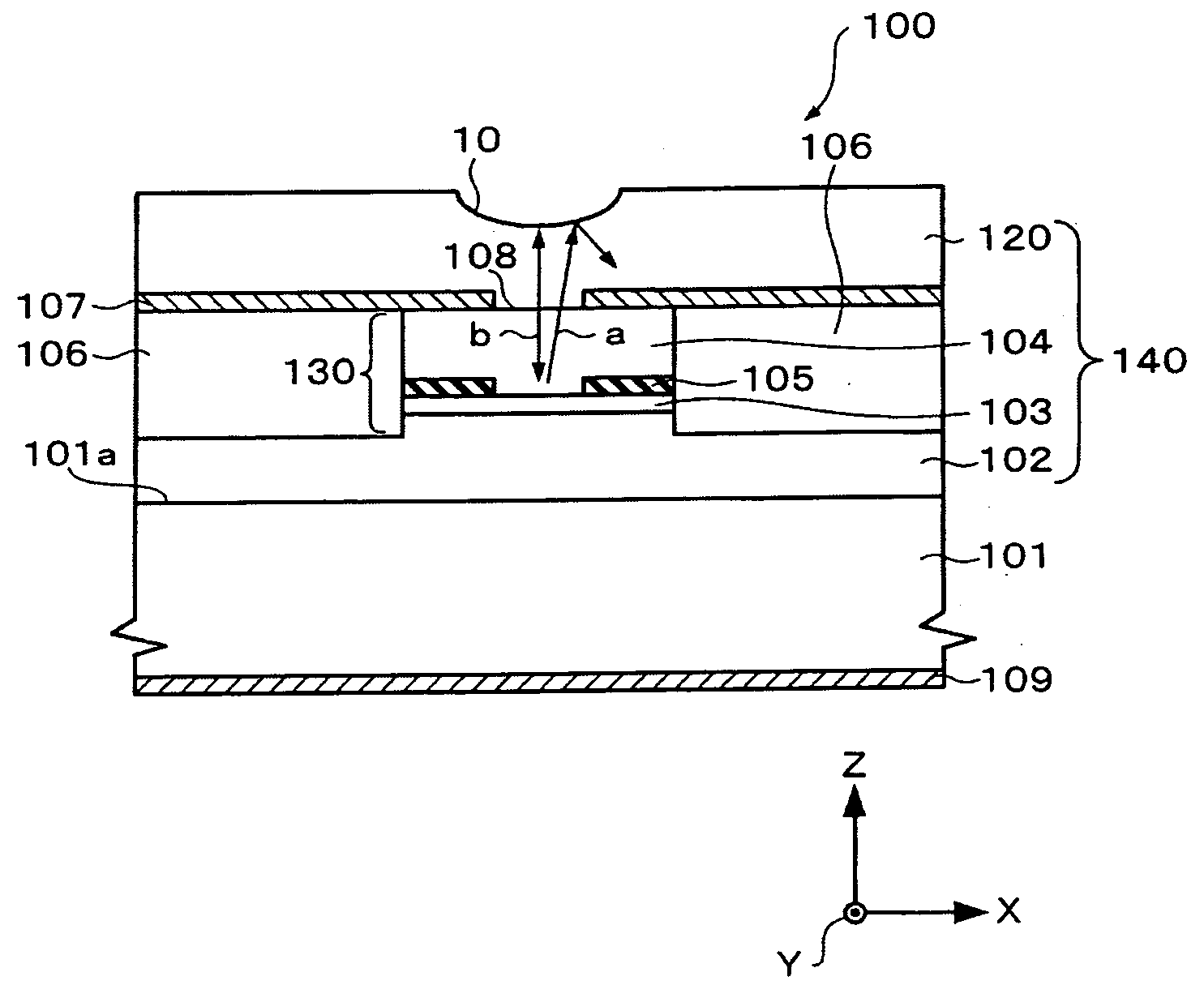
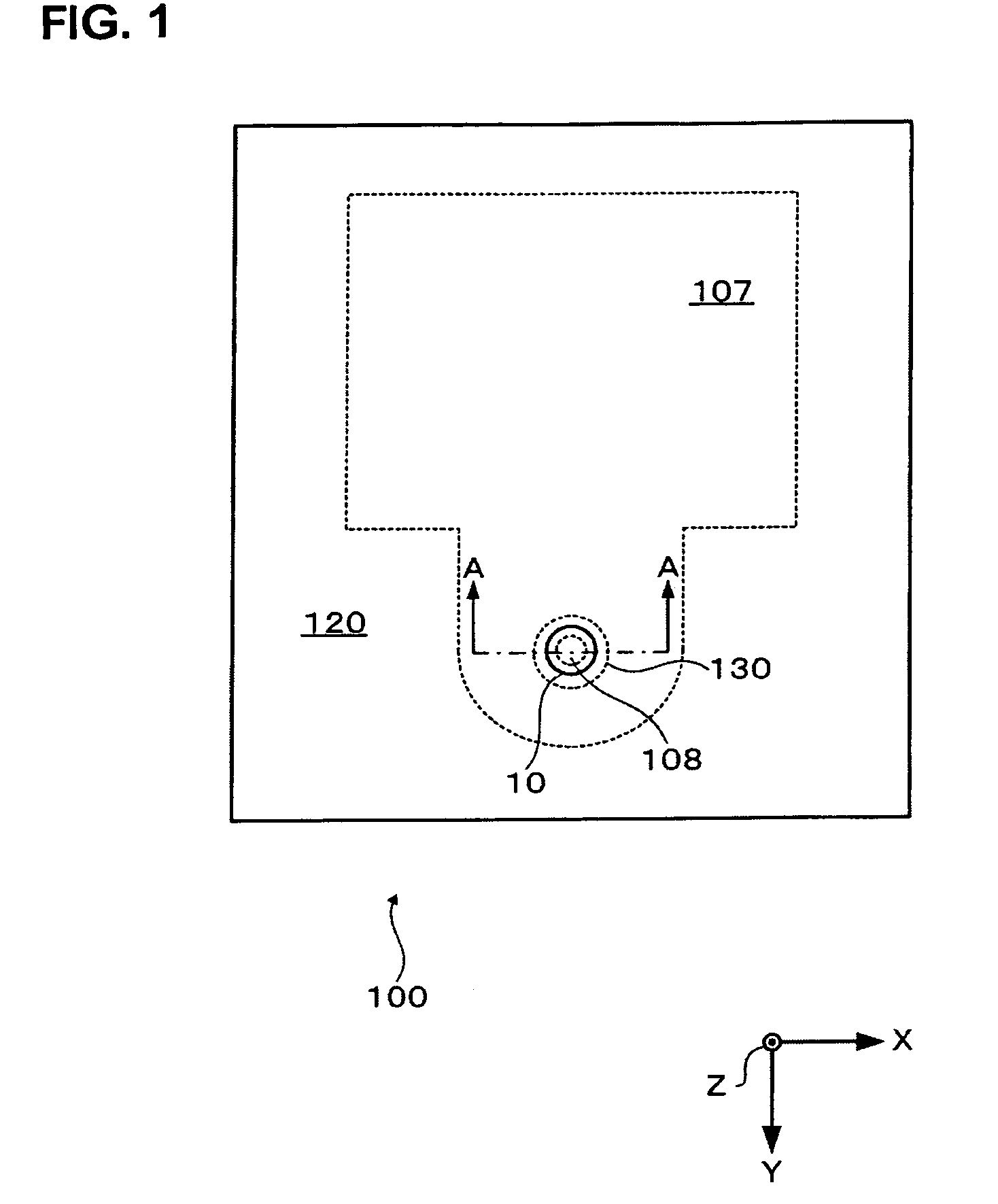
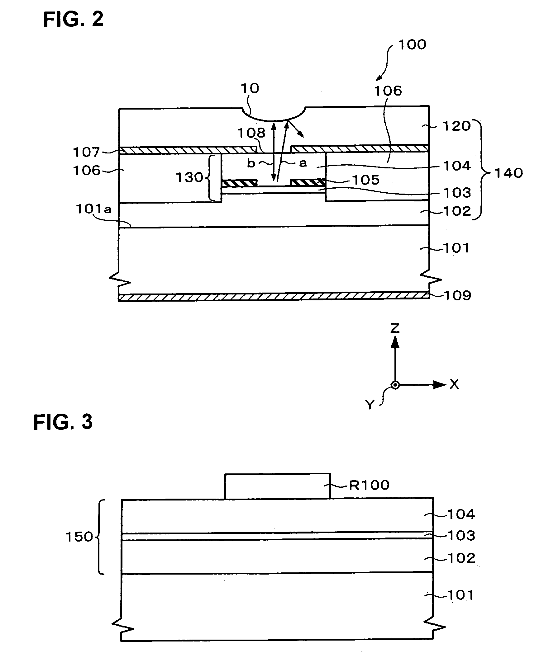
[0035]FIG. 1 is a schematic of a surface-emitting type semiconductor laser (hereinafter “surface emitting laser”) 100 in accordance with a first exemplary embodiment of the present invention. FIG. 2 is a schematic taken along a plane A-A of FIG. 1.
[0036] The surface emitting laser 100 according to the present exemplary embodiment includes, as shown in FIG. 1 and FIG. 2, a semiconductor substrate (a GaAs substrate in the present exemplary embodiment) 101, a vertical resonator (hereafter “resonator”) 140 formed on the semiconductor substrate 101, a first electrode 107 and a second electrode 109. The resonator 140 includes a first mirror 102, an active layer 103, a second mirror 104, and an optical path adjusting layer 120 including a concave curved surface 10.
[0037] Next, components of the surface-emitting laser 100 are described below.
[0038] The resonator140 may be formed, for example, from the first mirror 102 that is a distribu...
second exemplary embodiment
2. Second Exemplary Embodiment
2-1 Device Structure
[0084]FIG. 12 is a schematic of a surface-emitting type semiconductor laser 200 in accordance with a second exemplary embodiment of the present invention. It is noted that the same reference numerals are appended to components that are substantially the same as those of the surface-emitting type semiconductor laser 100 in accordance with the first exemplary embodiment, and their detailed description is omitted.
[0085] The surface-emitting laser 200 in accordance with the present exemplary embodiment has a structure different from that of the surface-emitting laser 100 of the first exemplary embodiment in that light emits from a back side 101b of a semiconductor substrate 101, a concave section 222 is disposed in the back surface 101b of the semiconductor substrate 101, an optical path adjusting layer 220 is embedded in the concave section 222, a second electrode 109 is formed on the same side of the semiconductor substrate 101 wher...
PUM
 Abstract
Description
Claims
Application Information


