Supercharge Your Innovation With Domain-Expert AI Agents!

Alignment and orientation features for a semiconductor package

a technology of aligning and orientation features and semiconductors, applied in semiconductor devices, semiconductor/solid-state device details, electrical apparatus, etc., can solve the problems of increasing difficulty in correctly distinguishing the first end of the lead finger of the lead frame from each other, the practicality of providing relatively small bonding pads, and the apparent electrical connection of such devices. achieve the effect of greater accuracy and greater reliability

Inactive Publication Date: 2005-07-07
MICRON TECH INC
View PDF12 Cites 2 Cited by
  • Summary
  • Abstract
  • Description
  • Claims
  • Application Information

AI Technical Summary

Benefits of technology

The use of eyepoint features enhances the accuracy of lead finger identification and orientation determination, leading to more reliable wire bonding and reduced production costs by minimizing errors and increasing production yields.

Problems solved by technology

Consequently, the problems associated with providing electrical connection to such devices are becoming increasingly apparent as will now be described in greater detail.
Consequently, since it is generally not practical to provide relatively small bonding pads with a distinctive shape, the first ends of the lead fingers are often formed with nearly identical geometries.
Thus, it is becoming increasingly difficult to correctly distinguish the first ends of the lead fingers of the lead frame from each other.
As a result, automated wire bonding systems are increasingly having difficulties in identifying the lead fingers to connect the appropriate wirebonds.
Furthermore, since the wire bonding system uses the position of the first end of the first lead finger to determine the positions of the first ends of the remaining lead fingers, the wire bonding system will incorrectly determine the positions of the first ends of the remaining lead fingers.
Consequently, since the wire bonding system is unable to properly connect the first and second bonding pads together, the semiconductor device will not provide the desired electrical characteristics.
Another shortcoming of prior art wire bonding systems is that they utilize lead frames that provide an insufficient indication of the orientation of the lead frame.
Since the lead frame is often formed in a symmetrical manner with respect to such a rotation, this problem may be overlooked by an observer responsible for visually inspecting the orientation of the lead frame.
Moreover, since the typical lead frame comprises a symmetrical shape with respect to the 180 degree rotation, the wire bonding system may not identify the incorrect orientation of the lead frame.
Consequently, since the first bonding pads are often disposed on the die in an asymmetrical manner and since the interconnecting wires are often installed with an asymmetrical configuration, it is likely that considerable time and materials will be wasted by the wire bonding system in a futile attempt to electrically couple the die with the lead frame.
Thus, since semiconductor devices formed in this manner lack the appropriate conducting paths that extend from the exposed leads, this problem results in increased failure rates, reduced production yields and increased production costs.

Method used


Image

  • Alignment and orientation features for a semiconductor package
  • Alignment and orientation features for a semiconductor package
  • Alignment and orientation features for a semiconductor package

Examples


Embodiment Construction

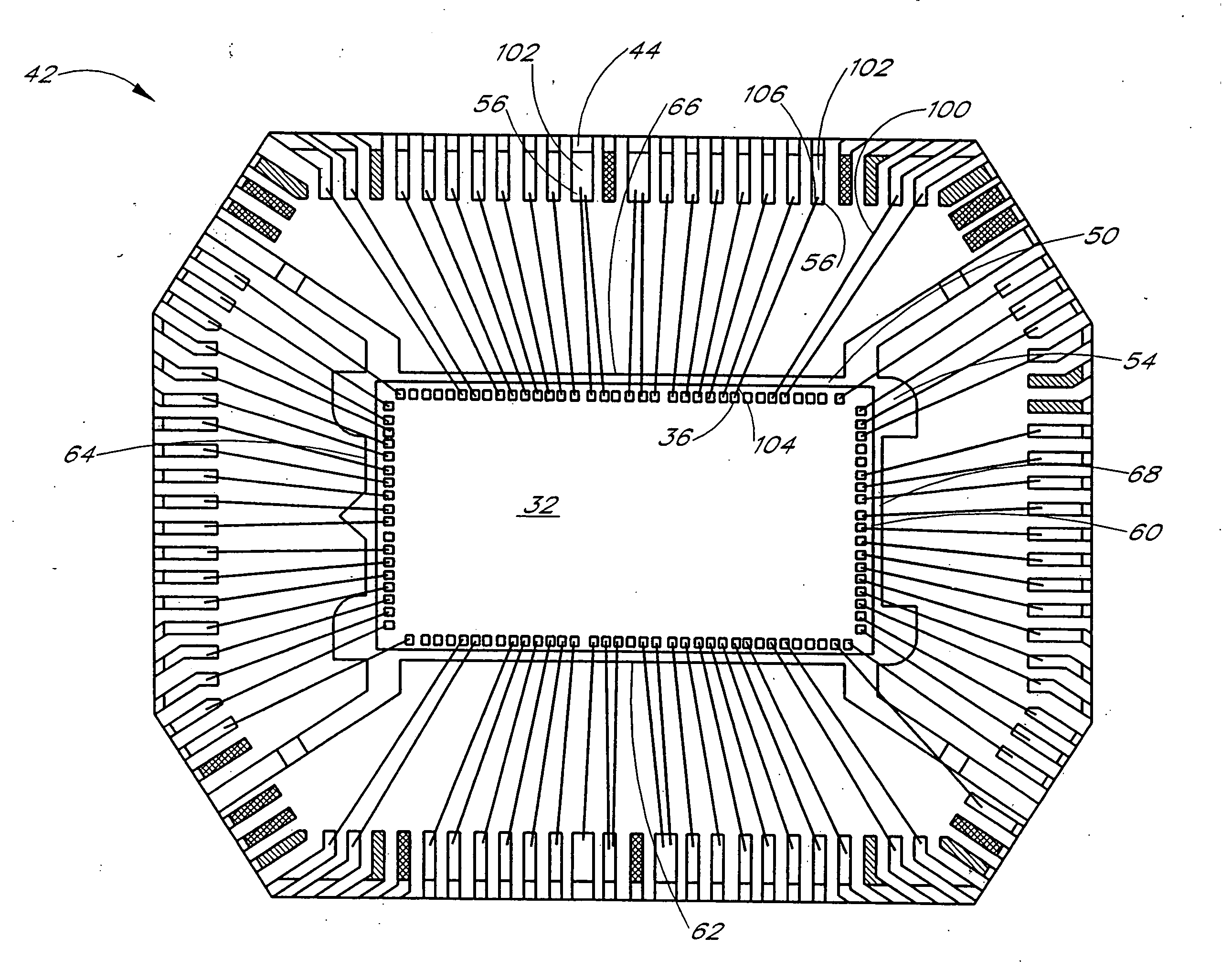
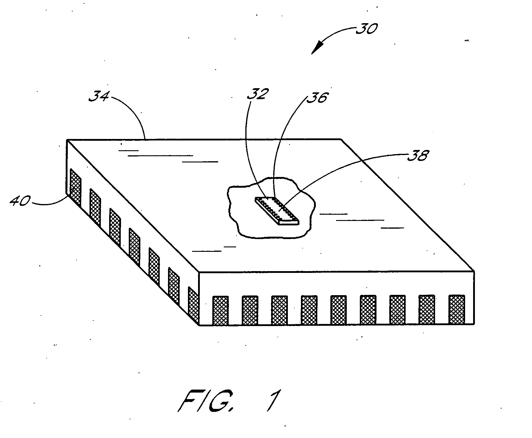
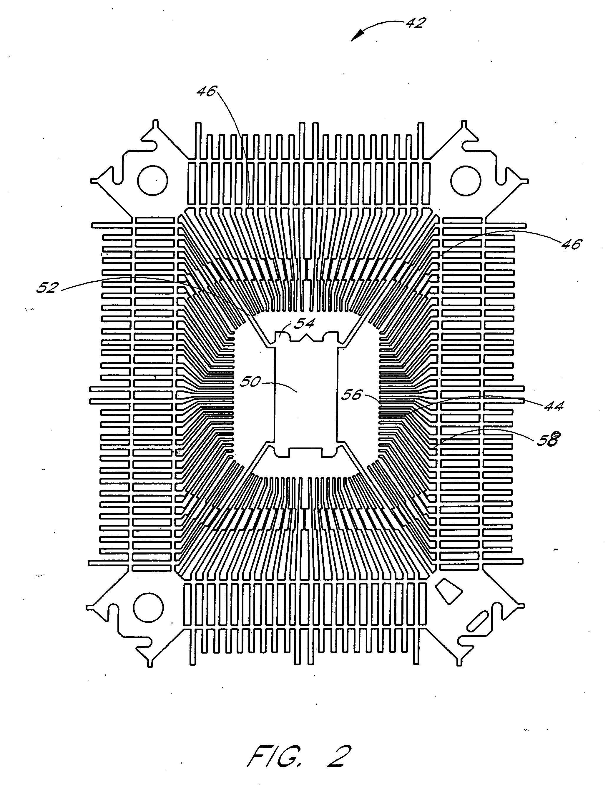
[0028] Reference will now be made to the drawings wherein like numerals refer to like parts throughout. In particular, FIG. 1 illustrates a semiconductor device 30 in accordance with one aspect of the present invention. The semiconductor device 30 comprises a known semiconductor die 32 housed within a known packaging material 34. The semiconductor die 32 comprises a preferred configuration of circuit elements that are interconnected so as to provide an electrical integrated circuit of any of a number of possible configurations. The semiconductor die 32 further comprises a first plurality of bonding pads 36 disposed a first surface 38 of the die 32 that electrically couple with a plurality of circuit nodes of the electrical circuit of the die 32.

[0029] As shown in FIG. 1, the semiconductor device 30 further comprises a plurality of exposed leads 40 that extend into the packaging material 34 so as to provide conducting paths that extend from the leads 40 toward the encapsulated die 3...


PUM


Abstract

A semiconductor device formed by an automated wire bonding system. The semiconductor device comprises a lead frame having a plurality of lead fingers and a die paddle, and a semiconductor die mounted to the die paddle. The die paddle comprises a plurality of eyepoint features that extend from the die. The die comprises a first plurality of bonding pads and the lead fingers comprise a second plurality of bonding pads. The first and second bonding pads are interconnected by a plurality of connecting wires which are installed by the automated wire bonding system. The wire bonding system obtains an image of the lead frame and identifies the eyepoint features of the die paddle within the image so as to more accurately determine the positions of the second wire bonding pads of the lead frame with respect to the wire bonding system

Description

RELATED APPLICATIONS [0001] This application is a continuation of U.S. patent application Ser. No. 10 / 439,369, filed May 16, 2003, which was a divisional of U.S. patent application Ser. No. 09 / 489,998, filed Jan. 21, 2000 (now U.S. Pat. No. 6,577,019, issued Jun.10, 2003), which are hereby incorporated in their entirety by reference herein.BACKGROUND OF THE INVENTION [0002] 1. Field of the Invention [0003] The present invention relates to semiconductor devices and, in particular, relates to a semiconductor device comprising a semiconductor die having a first plurality of bonding pads, and a lead frame having a second plurality of bonding pads, wherein the first bonding pads are connected to the second bonding pads by an automated wire bonding system. [0004] 2. Description of the Related Art [0005] Advances in semiconductor processing methods continually provide modular semiconductor devices with increased circuit density and, thus, increased functionality. As a result, such devices ...

Claims


Application Information

Patent Timeline
Patent Type & Authority Applications(United States)
IPC IPC(8): H01L23/495H01L23/544
CPCH01L23/49503H01L23/544H01L2924/01033H01L24/48H01L24/49H01L2223/54473H01L2224/48247H01L2224/49113H01L2224/49171H01L2924/01029H01L2924/01082H01L2924/14H01L2924/19041H01L2924/19043H01L2924/00H01L2224/05554H01L2924/00014H01L2224/45099H01L2224/05599
Inventor ROBERTS, STUART L.REEDER, WILLIAM J.MESS, LEONARD E.
Owner MICRON TECH INC
Features
  • R&D
  • Intellectual Property
  • Life Sciences
  • Materials
  • Tech Scout
  • Unparalleled Data Quality
  • Higher Quality Content
  • 60% Fewer Hallucinations
Learn More