Electronic device and method for producing the same

Inactive Publication Date: 2005-07-14
138 EAST LCD ADVANCEMENTS LTD
View PDF7 Cites 37 Cited by
  • Summary
  • Abstract
  • Description
  • Claims
  • Application Information

AI Technical Summary

Benefits of technology

[0077] When a pressure is applied during heating, the bond

Problems solved by technology

In the above-cited known method using crystal grain growth at the electrical interconnecting portion for MEMS (see, for example, PCT Japanese Translation Patent Publication No. 2003-519378, FIG. 1), manufacturing equipment such as vacuum equipment is required, thereby increasing the production cost

Method used


Image

  • Electronic device and method for producing the same
  • Electronic device and method for producing the same
  • Electronic device and method for producing the same

Examples


first embodiment

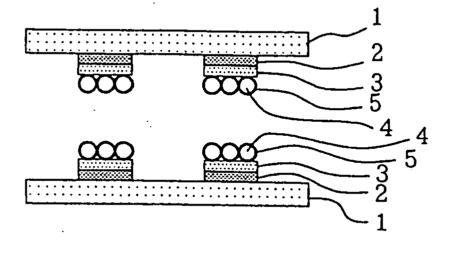
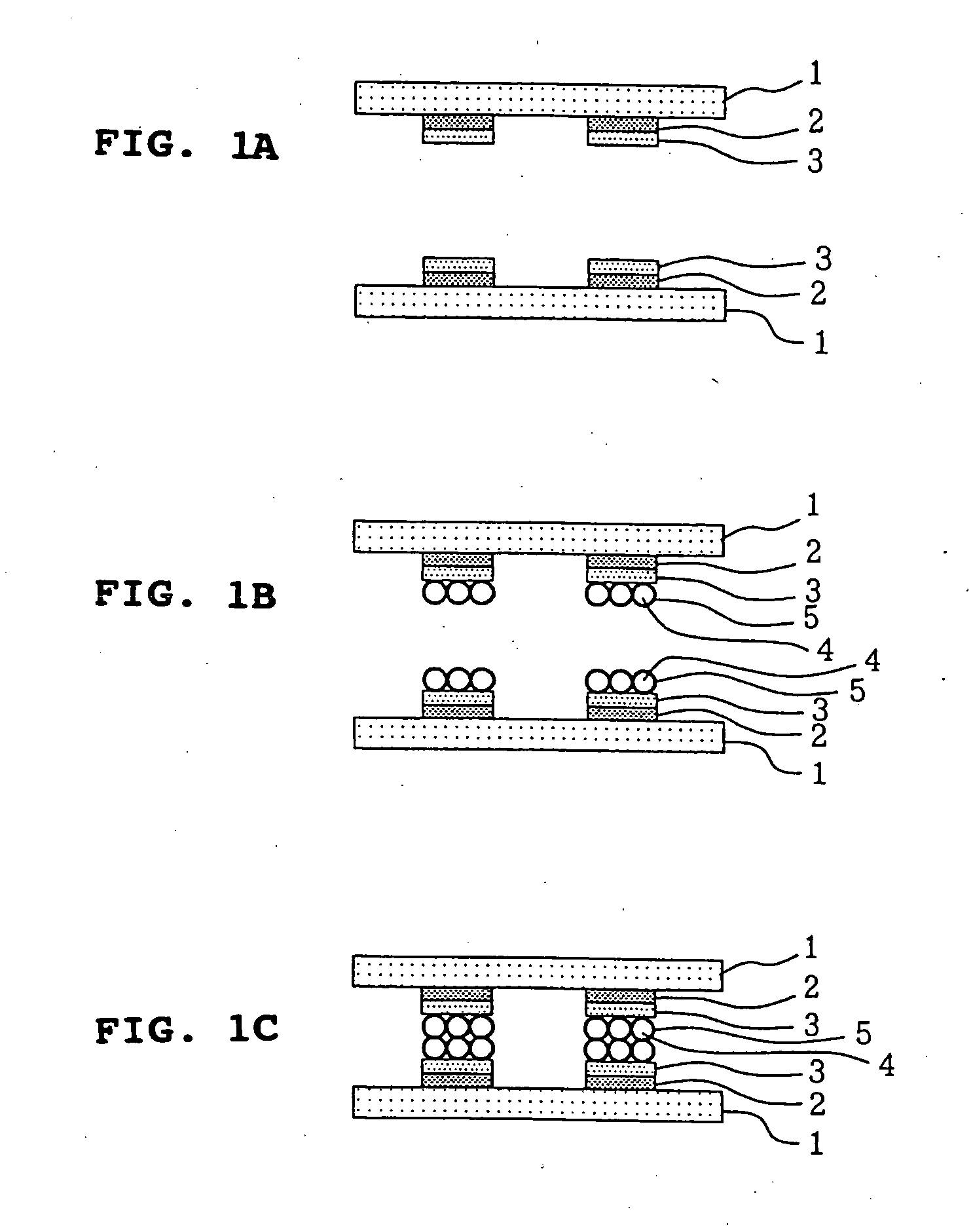
[0082]FIGS. 1A to 1C and FIGS. 2D and 2E are schematic cross-sectional views showing a production process of an electronic device according to a first embodiment of the present invention. Although two components are bonded in this embodiment shown in FIGS. 1A to 1C and FIGS. 2D and 2E, this process can be applied to bond at least three components, for example, to bond a plurality of semiconductor devices with a substrate. In addition, although FIGS. 1A to 1C and FIGS. 2D and 2E show two bonding portions, the number of bonding portions may be one or three or more. According to the present invention, examples of the electronic device include a circuit board bonded with a semiconductor device (i.e., integrated circuit (IC)), semiconductor devices bonded together, and micro electromechanical systems (MEMS).

[0083] Firstly, electrodes 2 are formed on two components 1. Receiving layers 3 are formed on the surfaces of the electrodes 2 (FIG. 1A). Examples of these components 1 include a cir...

second embodiment

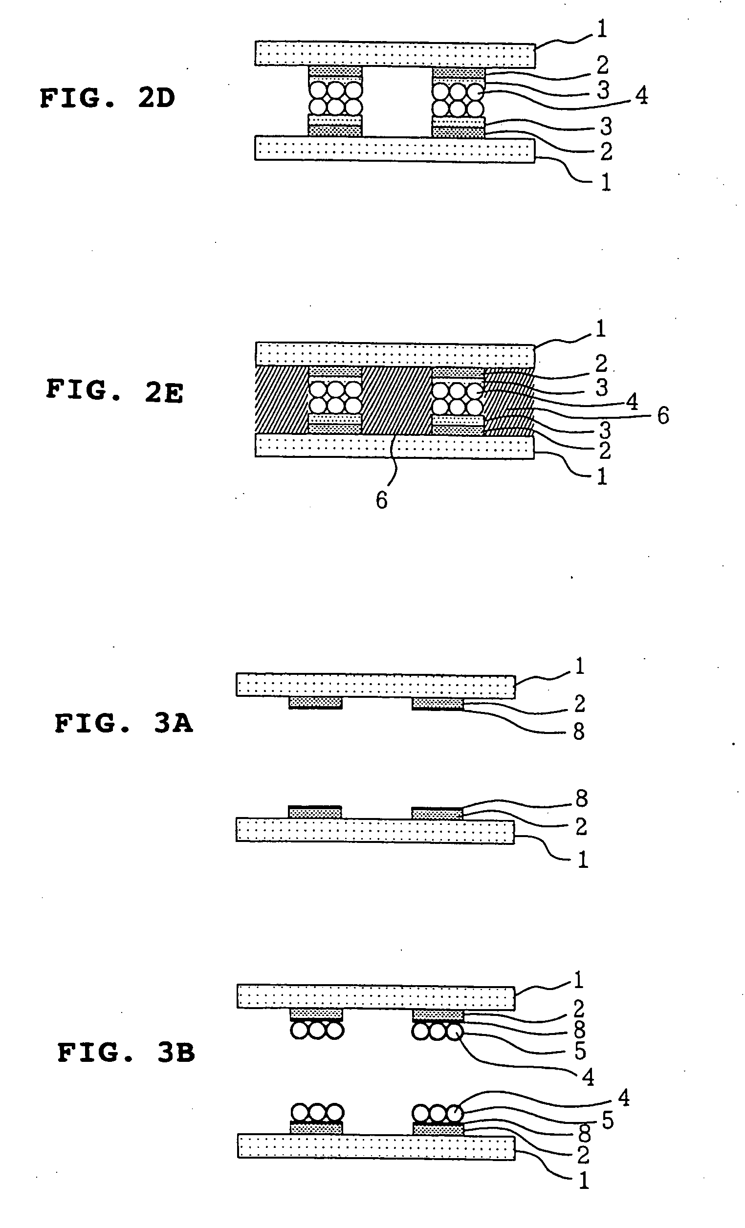
[0102]FIGS. 3A and 3B are schematic cross-sectional views showing a production process of an electronic device according to a second embodiment of the present invention. In this second embodiment, instead of the receiving layers 3 in the first embodiment, receiving structures 8 for holding nanoparticles 4 are formed on the surfaces of electrodes 2. In the manufacturing process in the second embodiment, the step shown in FIG. 1A in the first embodiment is replaced with the step shown in FIG. 3A, and the step shown in FIG. 1B in the first embodiment is replaced with the step shown in FIG. 3B. The subsequent steps are the same as those shown in FIG. 1C, FIG. 2D, and FIG. 2E. Other aspects are the same as those in the first embodiment, and the same elements as those in the first embodiment have the same reference numerals. The second embodiment will now be described.

[0103] Firstly, electrodes 2 are formed on both components 1. Receiving structures 8 are formed on the surfaces of the el...

third embodiment

[0108]FIGS. 4A and 4B are views showing examples of electronic equipment according to a third embodiment of the present invention. The electronic equipment shown in the third embodiment includes the electronic device produced by the methods for producing the electronic device described in the first embodiment and the second embodiment. FIG. 4A shows a notebook-size personal computer 100 as an example of the electronic equipment. FIG. 4B shows a cellular phone 200 as an example of the electronic equipment. The electronic devices shown in the first embodiment and the second embodiment can also be used in, for example, other household electronic appliances.


PUM


Abstract

An electronic device includes a plurality of components, nanoparticles to bond the components, and a receiving layer for holding the nanoparticles, the receiving layer being disposed on at least one of the bonded components. The electronic device may further include an electrode disposed on at least one of the plurality of components. The receiving layer is disposed on the surface of the electrode. Conductive particles etc. are mixed in the receiving layer.

Description

CROSS-REFERENCE TO RELATED APPLICATION [0001] The entire disclosure of Japanese Patent Application No. 2004-006426 filed Jan. 14, 2004 is hereby incorporated by reference. BACKGROUND OF THE INVENTION [0002] 1. Field of the Invention [0003] The present invention relates to an electronic device and a method for producing the same, and in particular, to an electronic device formed by bonding a plurality of components with nanoparticles and a method for producing the same. [0004] 2. Description of the Related Art [0005] In a known method using crystal grain growth at an electrical interconnecting portion for micro electro-mechanical systems (MEMS), a first layer of a MEMS device is electrically connected with a second layer thereof by growing conductive crystal grains between the first layer and second layer (see, for example, PCT Japanese Translation Patent Publication No. 2003-519378, FIG. 1). [0006] In a known printed circuit board and a method for producing the same, tin particles a...

Claims


Application Information

Patent Timeline
IPC IPC(8): H01L21/60H05K3/10H05K3/32
CPCB82Y30/00H01L2924/0105H01L24/81H01L2224/13099H01L2224/81801H01L2924/01002H01L2924/01009H01L2924/01012H01L2924/01013H01L2924/01015H01L2924/0102H01L2924/01029H01L2924/01033H01L2924/01047H01L2924/01056H01L2924/01078H01L2924/01079H01L2924/14H05K3/102H05K3/321H05K2201/0257H05K2201/10674H01L2924/01005H01L2924/01006H01L24/11H01L2224/11332H05K3/32
Inventor HASHIMOTO, NOBUAKI
Owner 138 EAST LCD ADVANCEMENTS LTD
Why Eureka
Try Eureka