Superconducting current limiting element

superconducting technology, applied in the direction of superconductor devices, superconductor emergency protection arrangements for limiting excess voltage/current, etc., can solve the problems of damage to the superconductor, superconductor cannot be used as a current limiting element, and large amount of joule heat generation

Inactive Publication Date: 2005-07-14
KK TOSHIBA
View PDF7 Cites 51 Cited by
  • Summary
  • Abstract
  • Description
  • Claims
  • Application Information

AI Technical Summary

Benefits of technology

[0017] A superconducting current limiting element according to an aspect of the present invention comprises: a parallel circuit including a first superconductor and a normal conductor connected in parallel; and a second superconductor connected in series to the parallel circuit and having a critical current value higher than that of the first superconductor, at least one of the normal conductor and the first superconductor, and the second superconductor being disposed on the same insulating substrate.

Problems solved by technology

However, a superconductor cannot be used as a current limiting element if it is simply connected in series in the electric power system, because it is easily damaged in this case.
It is considered that, if a high current not suppressed yet flows through the local normal-conducting region immediately after a current limiting operation is started, a very large amount of Joule heat is generated, which damages the superconductor.
Such thermal stress is also considered as a cause of damaging the superconductor.
However, the conventional resistive superconducting current limiting element shown in FIG. 1 also has a problem.
However, these methods require a coil for generating the magnetic field or a heater.
Therefore, it is difficult in these methods to make the current limiting element compact.
That is, the above current limiting element can reduce a time required for the whole superconductor to be converted into a normal conductor, but it cannot increase the resistance.

Method used


Image

  • Superconducting current limiting element
  • Superconducting current limiting element
  • Superconducting current limiting element

Examples


example 1

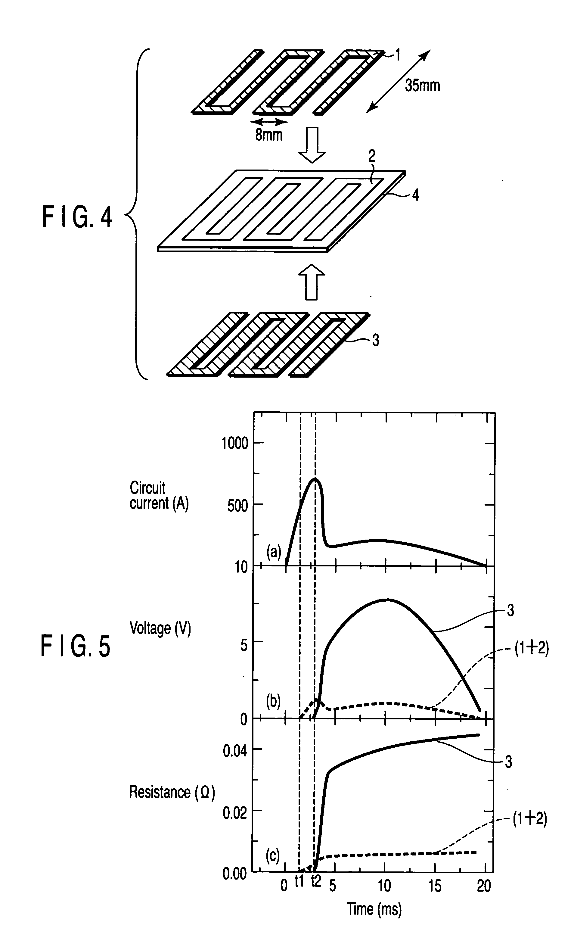
[0045]FIG. 3 is a perspective view of the superconducting current limiting element in this example. FIG. 4 is an exploded perspective view of the superconducting current limiting element in this example.

[0046] A normal conductor 2 made of a Ni thin film and processed into a meander shape was formed on one surface (upper surface) of an insulating substrate 4 made of sapphire having a thickness of 1 mm. A first superconductor 1 processed into a meander shape was formed on the normal conductor 2. In this case, a Y-based bulk superconductor was lapped into a plate having a thickness of 0.3 mm, and the plate was further processed into a meander-shaped strip having a width of 1 mm, and the resultant strip was used for the first superconductor 1. The total length of the first superconductor was about 200 mm. The first superconductor 1 was coated with a thin silver paste on one surface thereof, which was adhered to the normal conductor 2. A second superconductor 3 processed into a meander ...

example 2

[0054]FIG. 7 is a perspective view showing the upper surface of the superconducting current limiting element in this example. FIG. 8 is a perspective view showing the lower surface of the superconducting current limiting element in this example.

[0055] A Ni thin film was deposited on the upper surface of an insulating substrate 4 made of sapphire having a width of 5 cm, a length of 15 cm, and a thickness of 1 mm, and processed into a strip having a width of 3 cm and a length of 12 cm to form a normal conductor 2. As a first superconductor 1, a wire made of a Y-based superconducting thin film deposited on a metal tape having a thickness of 100 μm, a width of 1 cm, and a length of 12 cm was used. The metal tape having the first superconductor 1 thereon was adhered to the normal conductor 2 made of the Ni thin film using epoxy resin. As a second superconductor 3, a Y-based superconducting thin film deposited on CeO2 by an MOD method, which was epitaxially deposited on an R-plane sapphi...

example 3

[0062]FIG. 10 is a perspective view showing a superconductor conducting current limiting element in this example. FIG. 11 is an exploded perspective view showing the upper surface of the superconducting current limiting element in this example. FIG. 12 is an exploded perspective view showing the lower surface of the superconducting current limiting element in this example.

[0063] Example 3 is different from Example 2 in that, as a first superconductor 1, a Y-based superconducting thin film epitaxially deposited on CeO2 by evaporation, which was epitaxially deposited on a sapphire substrate having a thickness of 1 mm, a width of 1 cm, and a length of 12 cm, was used. Other constitution was similar to that of Example 2.

[0064] The first superconductor 1 had Ic of about 130 Å and the second superconductor 3 had Ic of about 200 Å, respectively, under the liquid nitrogen temperature. In this Example 3, the Ic of the first superconductor 1, which determines a current capacity of a current...


PUM

PropertyMeasurementUnit
thicknessaaaaaaaaaa
widthaaaaaaaaaa
thicknessaaaaaaaaaa

Abstract

A superconducting current limiting element has a parallel circuit including a first superconductor and a normal conductor connected in parallel, and a second superconductor connected in series to the parallel circuit and having a critical current value higher than that of the first superconductor. Further, at least one of the normal conductor and the first superconductor, and the second superconductor are disposed on the same insulating substrate.

Description

CROSS-REFERENCE TO RELATED APPLICATIONS [0001] This application is based upon and claims the benefit of priority from prior Japanese Patent Application No. 2004-003570, filed Jan. 9, 2004, the entire contents of which are incorporated herein by reference. BACKGROUND OF THE INVENTION [0002] 1. Field of the Invention [0003] The present invention relates to a superconducting current limiting element instantaneously suppresses an excessive current, such as a short circuit current transmitting electric power transmission lines, utilizing transition of a superconductor from a superconducting state to a normal-conducting state. [0004] 2. Description of the Related Art [0005] A current limiting element is capable of conducting a current having a certain value or less while hardly generating a loss, but, when a high current is to be flowed, generates impedance to suppress the current. The current limiting element is applied to electric power equipment required to suppress a fault current due...

Claims


Application Information

Patent Timeline
Patent Type & Authority Applications(United States)
IPC IPC(8): H01B1/00H01L39/16H01B12/06H01B13/00H02H9/02
CPCH01L39/16H10N60/30
Inventor KUBOTA, HIROSHI
Owner KK TOSHIBA
Why Eureka
Try Eureka