
Photomask and method of controlling transmittance and phase of light using the photomask

a technology of photomask and transmittance, applied in the field of photomask, can solve the problems of limiting the effect of high-resolution photolithography, unable to control the phase and transmittance, and unable to control the light transmittance and not the phase, so as to achieve the effect of improving the cd distribution by controlling the transmittan

Active Publication Date: 2005-07-21
SAMSUNG ELECTRONICS CO LTD
View PDF2 Cites 6 Cited by
  • Summary
  • Abstract
  • Description
  • Claims
  • Application Information

AI Technical Summary

Benefits of technology

[0010] The present invention provides a photomask capable of improving a CD distribution by controlling transmittance. A modified illumination effect is obtained for a photolithography process with respect to both the transmittance and phase of light.
[0011] The present invention also provides a method of controlling transmittance and phase of light, thereby improving CD distribution using a lattice structure on the back face of a photomask. The lattice structure of the present invention forms a multiphase diffraction optical element.

Problems solved by technology

The efficacy of high resolution photolithography is limited, however, by a mask error enhancement factor (MEEF).
Although modified illumination is obtained by forming the lattice structure on the back face of the photomask, this method fails to control the phase and transmittance.
This method, however, only controls the transmittance of light and not the phase.
Therefore, when transcribing a complicated variety of patterns on a wafer using an exposure process, pattern defects often occur due to transmittance distribution.
However, noise is caused due to limited diffraction efficiency, which has a negative effect on the formation of patterns on a wafer.

Method used


Image

  • Photomask and method of controlling transmittance and phase of light using the photomask
  • Photomask and method of controlling transmittance and phase of light using the photomask
  • Photomask and method of controlling transmittance and phase of light using the photomask

Examples


Embodiment Construction

[0047] The present invention will now be described more fully with reference to the accompanying drawings, in which several exemplary embodiments of the present invention are shown. In the drawings, the thickness of layers and regions is exaggerated for clarity. Throughout the drawings and the written description, like reference numerals are used to refer to like elements.

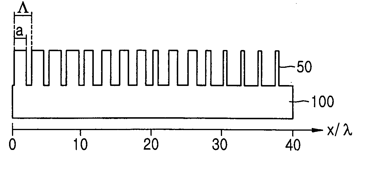
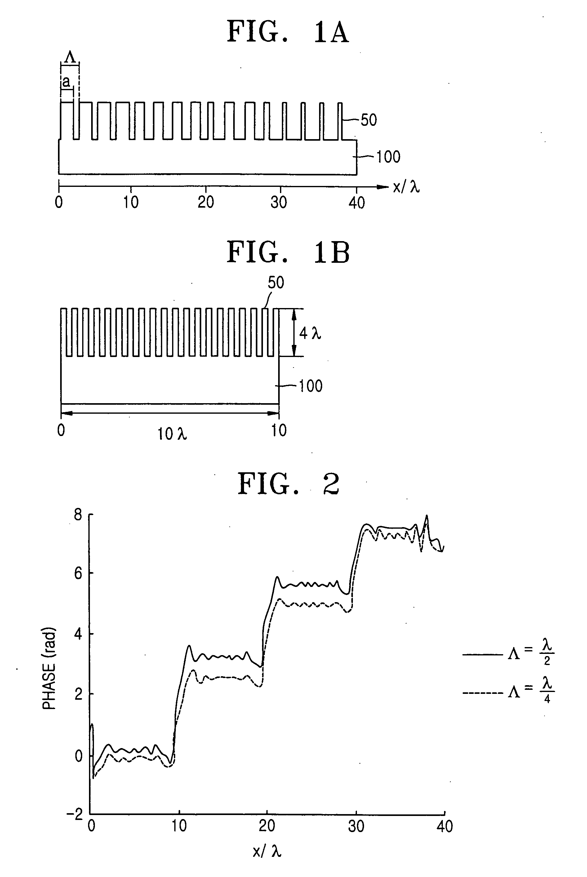
[0048]FIG. 1A is a cross-sectional view illustrating a lattice structure comprising lattices having different duty ratios. FIG. 1A is used to explain a principle related to the present invention.

[0049] Referring to FIG. 1A, a plurality of lattices 50 is formed by selectively etching the back face of transparent substrate 100 in order to form part of a photomask. A tilt angle for lattices 50 is 0°. In other words, all lattices are formed in a uniform direction.

[0050] Each of the lattices 50 is a binary lattice, i.e., the teeth and the corresponding adjacent spaces within lattices 50 have equal depths. A pitch “Λ”...


PUM

PropertyMeasurementUnit
tilt angleaaaaaaaaaa
transparentaaaaaaaaaa

Abstract

A photomask and a method of controlling a transmittance and phase of light using the photomask are disclosed. The photomask comprises a transparent substrate, and a plurality of lattices formed on the back face of the transparent substrate. The plurality of lattices are binary lattices, each having a duty ratio and a tilt angle. The duty ratio and tilt angle are controlled together in order to simultaneously control transmittance and phase of light transmitted through the photomask.

Description

BACKGROUND OF THE INVENTION [0001] 1. Field of the Invention [0002] The present invention relates generally to a photomask and a method of controlling the transmittance and phase of light using the photomask. More particularly, the present invention relates to a photomask controlling the transmittance and phase of light using lattice structures wherein a pitch is shorter than a wavelength of the light. [0003] A claim of priority is made to Korean Patent Application No. 2004-4419, filed Jan. 20, 2004, the disclosure of which is incorporated herein by reference in its entirety. [0004] 2. Description of the Related Art [0005] High resolution photolithography is generally used in manufacturing highly integrated semiconductor integrated circuits. The efficacy of high resolution photolithography is limited, however, by a mask error enhancement factor (MEEF). Since a photolithography process used to etch a wafer generally requires a critical dimension (CD) distribution that cannot be provi...

Claims


Application Information

Patent Timeline
Patent Type & Authority Applications(United States)
IPC IPC(8): H01L21/027G03F1/00G03F1/14G03F9/00G06K9/36
CPCG03F1/0084G03F1/14G03F1/38G03F1/34G03F1/26G03F1/50G03F1/62G03F1/80
Inventor PARK, JIN-HONGCHOI, SEONG-WOON
Owner SAMSUNG ELECTRONICS CO LTD
Learn More