Method of forming contact plug on silicide structure

a technology of contact plug and silicide structure, which is applied in the direction of semiconductor/solid-state device manufacturing, basic electric elements, electric apparatus, etc., can solve the problems of contact resistivity (rc) failure—essentially an open circuit, and achieve the effect of reducing contact rc failure, reducing reaction time, and increasing manufacturing process yield

Inactive Publication Date: 2005-07-21
TAIWAN SEMICON MFG CO LTD
View PDF31 Cites 17 Cited by
  • Summary
  • Abstract
  • Description
  • Claims
  • Application Information

AI Technical Summary

Benefits of technology

[0010] The new method of manufacturing a semiconductor device minimizes reactions between the nickel silicide contact regions during opening of contact holes or tunnels during the formation of contact plugs thereto. The process thereby reduces contact Rc failures and increases the yield of the manufacturing process.

Problems solved by technology

A problem arises, however, when opening contact holes to nickel silicide contact regions using prior art processes.
These processes typically use CF based etchants, such as CHxFy / O2 and CxFy / O2 and it is believed that the O2, F and / or CO components of either or both of the photoresist removal etchant or the etch stop layer removal etchants react with the nickel silicide contact regions, resulting in contact resistivity (Rc) failure—essentially an open circuit.

Method used


Image

  • Method of forming contact plug on silicide structure
  • Method of forming contact plug on silicide structure
  • Method of forming contact plug on silicide structure

Examples


Embodiment Construction

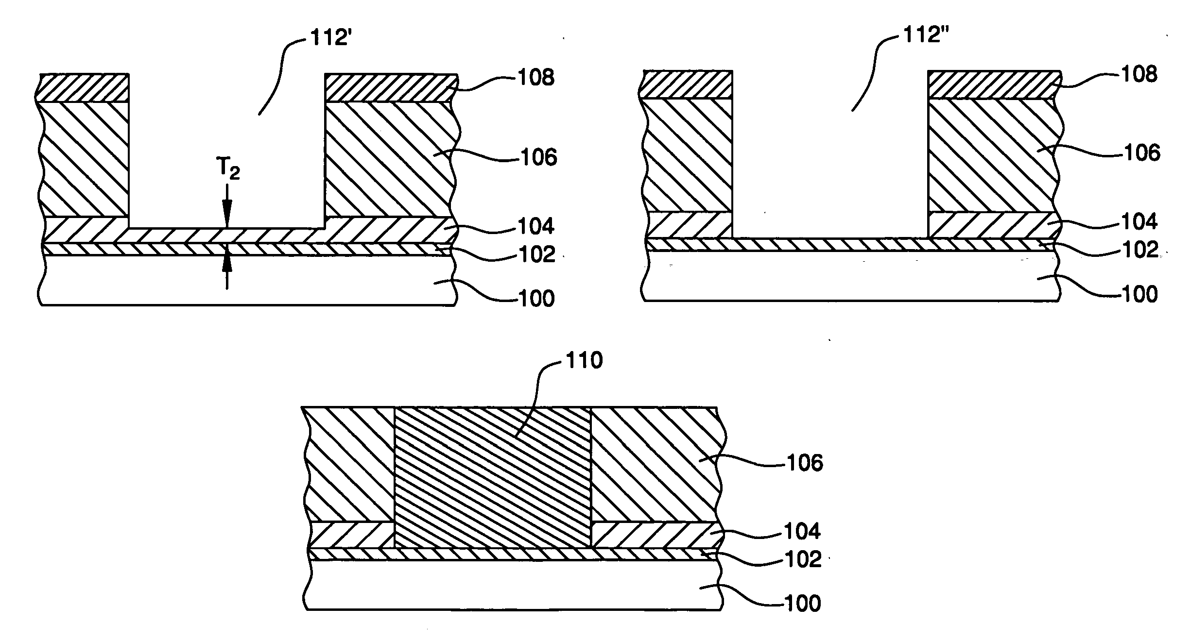
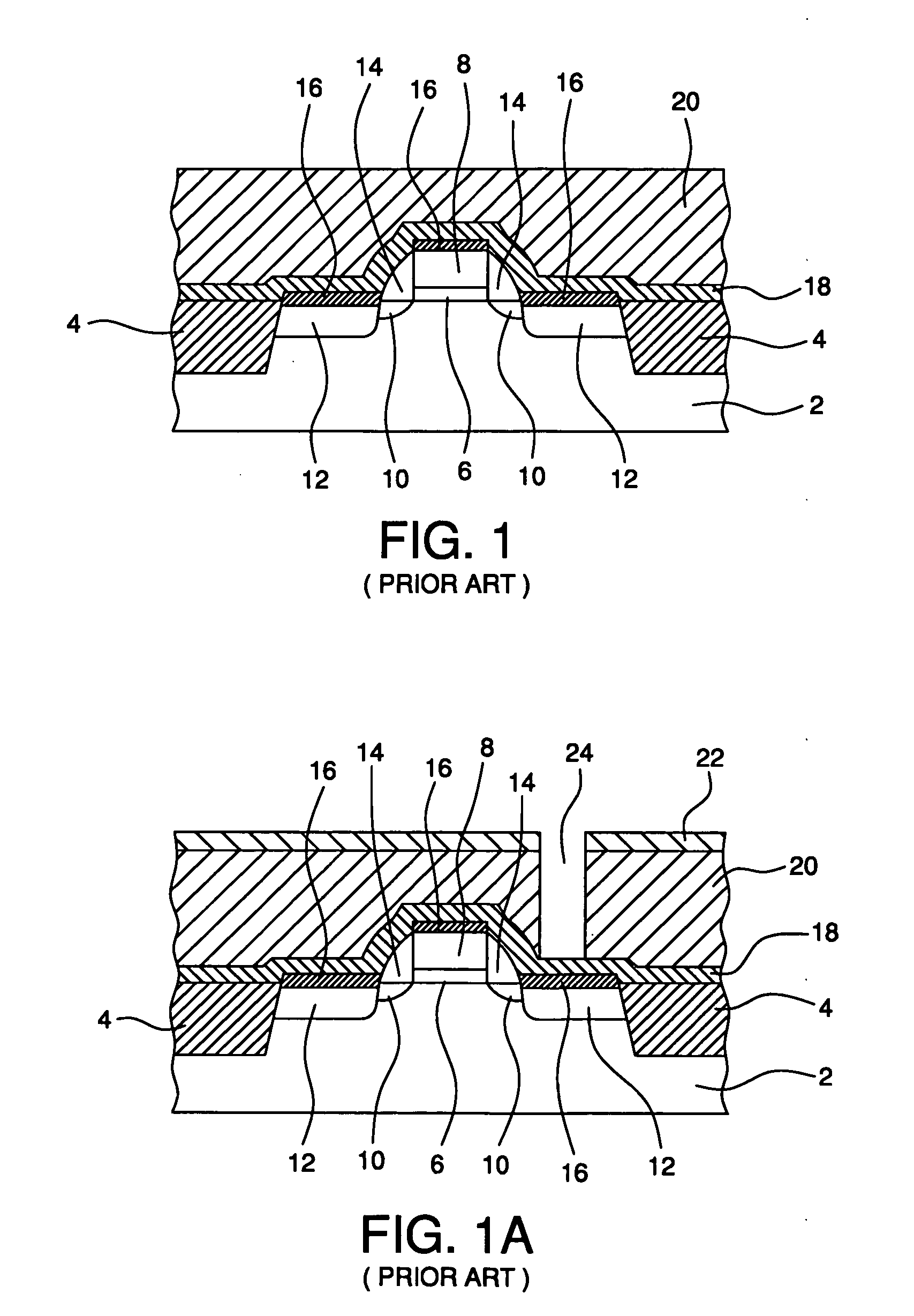
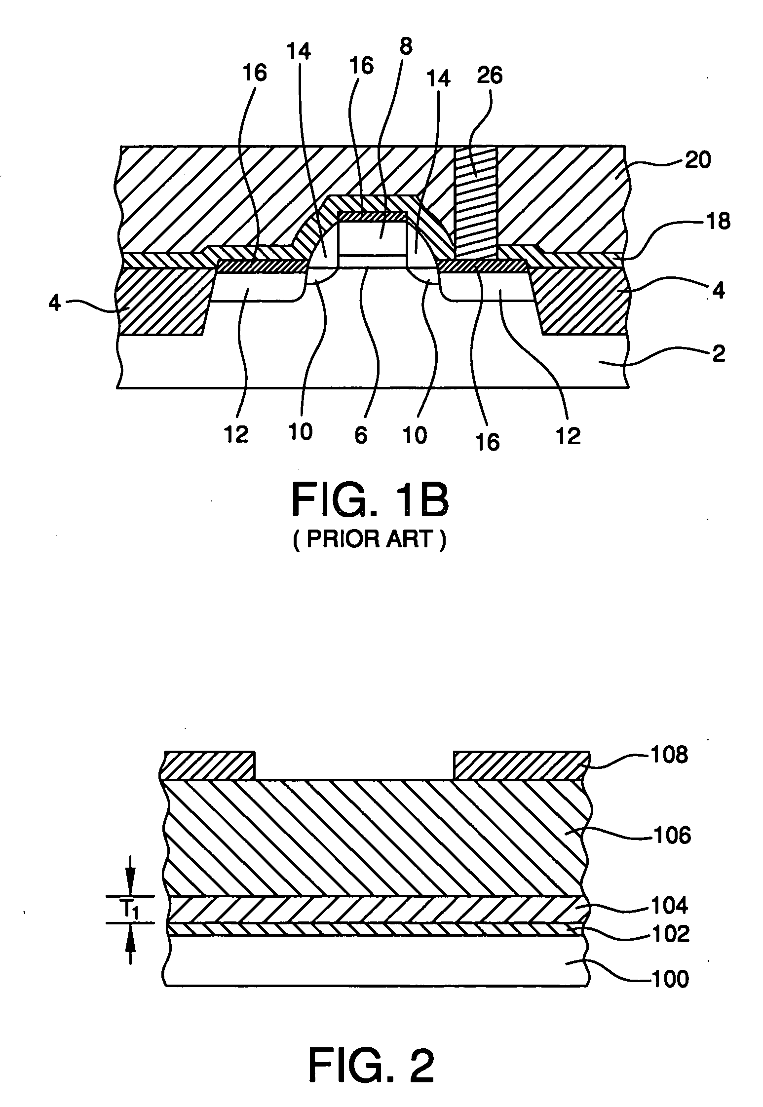
[0017] A new method of manufacturing an integrated circuit, including a new method of opening a contact hole to a contact region of a semiconductor device, is described hereafter in connection with FIGS. 2-4D. For ease of illustration, the method is described using enlarged views of contact regions of a semiconductor element without illustrating the complete element structure, and it should be understood that these views are only partial views of a complete structure, such as the MOS transistor device shown and described in connection with FIG. 1, a CMOS device, a capacitor or other semiconductor element.

[0018]FIGS. 2-2C illustrate a first exemplary method of forming a contact to a metal silicide region, preferably a nickel silicide region. Referring first to FIG. 2, a metal silicide contact region 102 is formed on a semiconductor substrate 100, such as a silicon, germanium or silicon on insulator (SOI) substrate. The metal silicide region 102 typically is formed over a source or d...


PUM


Abstract

A method of manufacturing a semiconductor device is provided comprising the steps of: (a) forming a semiconductor element on a substrate, the semiconductor element having at least one nickel silicide contact region, a first etch stop layer formed over the element and an insulating layer formed over the first etch stop layer; (b) forming an opening through the insulating layer over the contact region at least to the first etch stop layer; (c) removing a portion of the first etch stop layer contacting a selected contact region using a process that does not substantially oxidize with the contact region, to form a contact opening to the contact region; and (d) filling the contact opening with conductive material to form a contact.

Description

CROSS-REFERENCE TO RELATED APPLICATION [0001] This Application is a Continuation-in-Part of U.S. patent application Ser. No. 10 / 265,937 to Chii-Ming Wu et al., entitled “Method of Forming Contact Plug on Silicide Structure”, filed Oct. 7, 2002, now U.S. Pat. No. ______, the entirety of which is hereby incorporated by reference herein.FIELD OF THE INVENTION [0002] The present invention relates to methods of fabricating integrated circuits, and more particularly to methods of forming contact plugs in integrated circuit structures. BACKGROUND OF THE INVENTION [0003] A prior art method of forming a contact plug to a gate, source or drain region of a MOS device is provided in connection with FIGS. 1-1B. A MOS device structure is shown in FIG. 1. Methods for fabricating the structure of FIG. 1 are well known in the art of integrated circuit fabrication, as described in, for example, U.S. Pat. No. 6,232,224 to Inoue and U.S. Pat. No. 6,350,636 to Lee et al., the entirety of which are hereb...

Claims


Application Information

Patent Timeline
Patent Type & Authority Applications(United States)
IPC IPC(8): H01L21/311H01L21/60H01L21/768
CPCH01L21/31105H01L21/31116H01L21/76832H01L21/76829H01L21/76802
Inventor WU, CHII-MINGCHANG, CHIH-WEISHUE, SHAU-LINHSU, JU-WANGTSAI, MING-HUAN
Owner TAIWAN SEMICON MFG CO LTD
Why Eureka
Try Eureka