Megasonic cleaning using supersaturated cleaning solution

a technology of cleaning solution and supersaturated solution, which is applied in the direction of electrostatic cleaning, cleaning process and apparatus, electrical apparatus, etc., can solve the problems of increasing the likelihood of device failure, contaminating particle on a wafer occupying a greater percentage of the device's surface area, and increasing the cleaning requirements. strict, to achieve the effect of promoting particle removal

Inactive Publication Date: 2005-07-28
AKRION TECH
View PDF18 Cites 12 Cited by
  • Summary
  • Abstract
  • Description
  • Claims
  • Application Information

AI Technical Summary

Benefits of technology

[0023] In another aspect, the invention is a method of cleaning at least one semiconductor wafer comprising: (a) positioning a semiconductor wafer in a process chamber; (b) supplying a solution to the process chamber so as to contact the substrate, the solution comprising a cleaning liquid and a first and second gases dissolved in the cleaning liquid, wherein the first gas promotes particle removal from the wafer and the second gas protects the wafer from damage resulting from acoustical energy; and (c) applying acoustical energy through the solution and to the wafer to clean the wafer.

Problems solved by technology

Moreover, as semiconductor devices become more miniaturized and complex due to end product needs, the cleanliness requirements have become more stringent.
First, as devices become miniaturized, a contaminating particle on a wafer will occupy a greater percentage of the device's surface area.
This increases the likelihood that the device will fail.
Second, as devices become more complex, the raw materials, time, equipment, and processing steps necessary to make these devices also become more complex and more expensive.
As a result, the cost required to make each wafer increases.
However, it has been discovered that applied megasonic energy can also damage the semiconductor devices being cleaned.
The composition of the cleaning solution, including the quantity and composition of any gas dissolved in the cleaning solution, used in a megasonic cleaning process can affect cleaning efficiency and the amount of damage caused to the wafer.
The prior art teaches that cleaning solutions containing supersaturated levels of gas are undesirable for wafer cleaning processes.
The '626 patent further teaches that too much gas in solution can create defects in silicon surfaces.
The '891 patent attributes poor cleaning efficiency at supersaturated conditions to the formation of excessive gas bubbles in the solution that absorb the megasonic energy before it reaches the wafer surface.
U.S. Pat. No. 6,039,814 (the “'814 patent”) teaches that minute bubbles within the cleaning solution disrupt the propagation of sound, resulting in reduced cleaning efficiency.

Method used


Image

  • Megasonic cleaning using supersaturated cleaning solution
  • Megasonic cleaning using supersaturated cleaning solution
  • Megasonic cleaning using supersaturated cleaning solution

Examples


Embodiment Construction

[0030] The, described embodiments of the megasonic cleaning method of the present invention have several features, no single one of which is solely responsible for the desirable attributes. Without limiting the scope of this method as expressed by the claims that follow, its more prominent features will now be discussed.

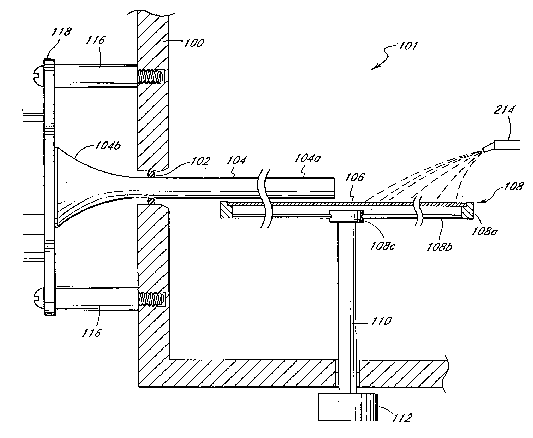
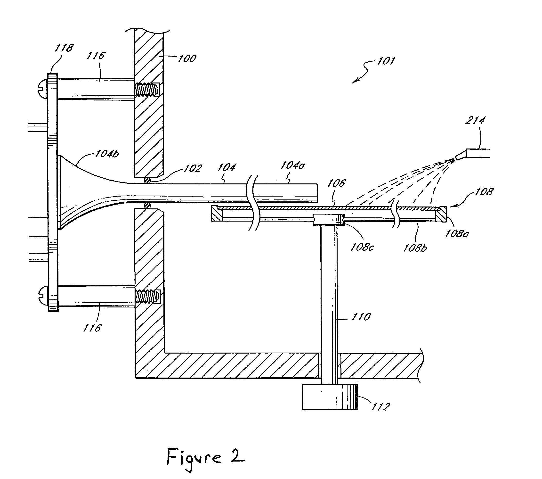
[0031] Efficiently cleaning semiconductor wafers using applied megasonic energy requires a proper concentration of dissolved gas in the cleaning solution. However, contrary to the teachings of the prior art, optimum cleaning with no wafer damage results from using a cleaning solution having a supersaturated concentration of dissolved gas. The methods of the present invention described herein are effective for cleaning wafers using both immersion and non immersion cleaning techniques. The wafer or wafers being cleaned may be immersed in cleaning solution or, alternatively, cleaning solution may be applied to the wafer surface as a thin film, by such means as spraying...


PUM

PropertyMeasurementUnit
wave lengthaaaaaaaaaa
temperatureaaaaaaaaaa

Abstract

A method and system for the megasonic cleaning of one or more substrates that reduces damage to the substrate(s) resulting from the megasonic energy. The substrates are supported in a process chamber and contacted with a cleaning solution comprising a cleaning liquid having carbon dioxide gas dissolved in the cleaning liquid in such amounts that the carbon dioxide gas is at a supersaturated concentration for the conditions within the process chamber. Megasonic energy is then transmitted to the substrate. The cleaning solution provides protection from damage resulting from the application of megasonic/acoustical energy. In another aspect, the invention is a system for carrying out the method. The invention is not limited to carbon dioxide but can be used in conjunction with any gas that, when so dissolved in a cleaning liquid, protects substrates from being damaged by the application of megasonic/acoustical energy.

Description

CROSS-REFERENCE TO RELATED APPLICATIONS [0001] This application claims the benefit of U.S. Provisional Application 60 / 477,602, filed Jun. 11, 2003, which is hereby incorporated by reference in its entirety.FIELD OF THE INVENTION [0002] The present invention relates generally to the methods, apparatus, and systems for substrate processing / manufacturing, and specifically to methods, apparatus, and systems for cleaning semiconductor wafers using applied megasonic energy. BACKGROUND OF THE INVENTION [0003] In the manufacture of semiconductors, semiconductor devices are produced on thin disk-like objects called wafers. Generally, each wafer contains a plurality of semiconductor devices. The importance of minimizing contaminants on the surface of these wafers during production has been recognized since the beginning of the industry. Moreover, as semiconductor devices become more miniaturized and complex due to end product needs, the cleanliness requirements have become more stringent. Thi...

Claims


Application Information

Patent Timeline
Patent Type & Authority Applications(United States)
IPC IPC(8): B08B3/00B08B7/00
CPCB08B3/12Y10S438/906H01L21/67051
Inventor FRANKLIN, COLE S.WU, YIFRASER, BRIAN
Owner AKRION TECH
Why Eureka
Try Eureka