

Array substrate for a liquid crystal display device and manufacturing method of the same
a liquid crystal display and substrate technology, applied in semiconductor devices, instruments, optics, etc., can solve the problem of ineffective adjustment of offset voltage vsub>p/sub>
- Summary
- Abstract
- Description
- Claims
- Application Information
AI Technical Summary
Problems solved by technology
Method used
Image

Examples
first embodiment
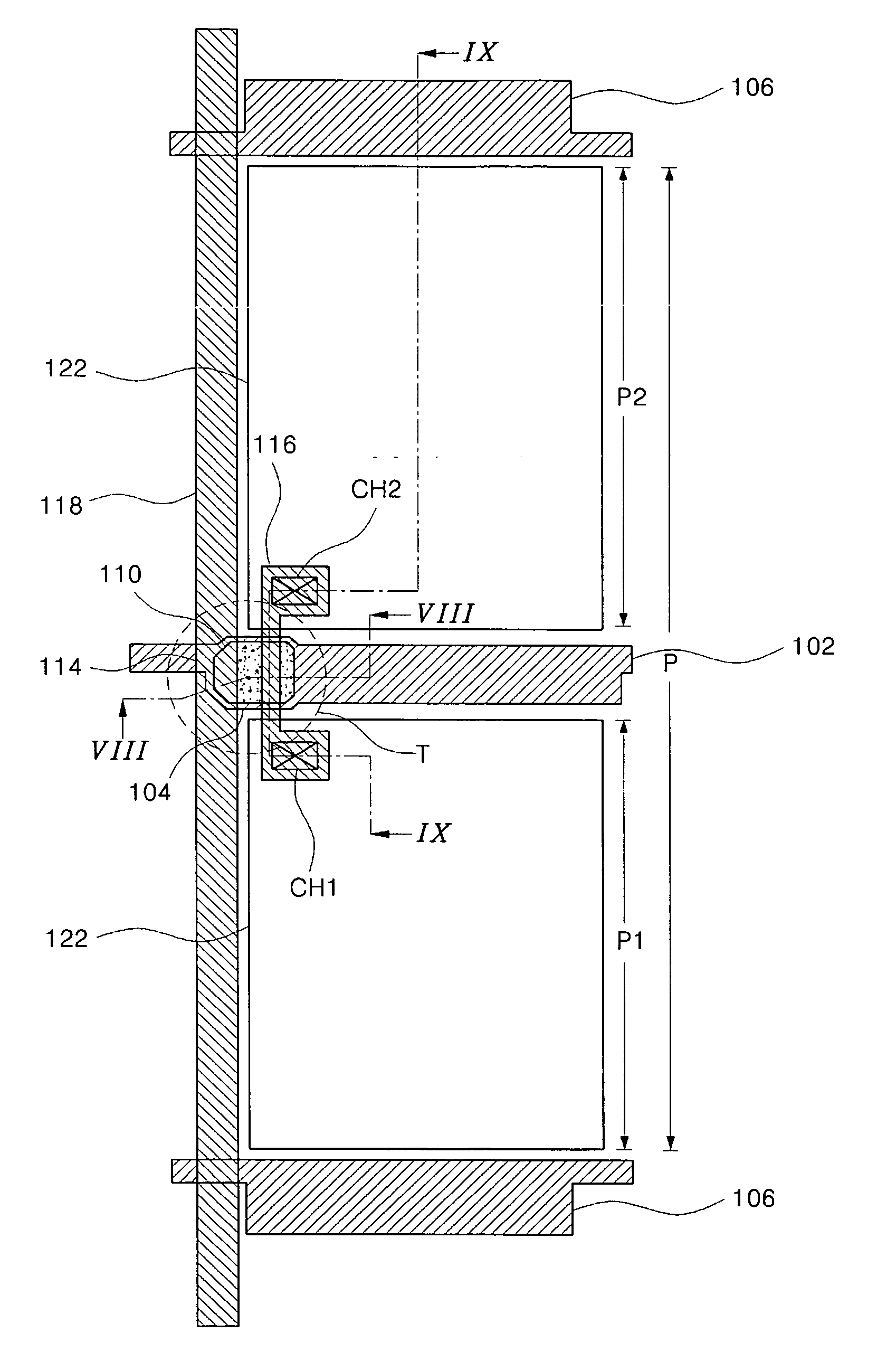
[0054]FIG. 7 is a plan view of an array substrate for an LCD device according to the present invention, and the array substrate includes the above-mentioned structure of the thin film transistor.
[0055] As shown in FIG. 7, a gate line 102 is formed in a first direction, and two common lines 106 parallel to the gate line 102 are formed such that the gate line 102 is disposed between the common lines 106. A data line 118 is formed in a second direction perpendicular to the first direction. The data line 118 crosses the gate line 102 and the common lines 106 to define a pixel region P, which includes a first region P1 and a second region P2 adjacent to each other in the second direction. The gate line 102 goes across a middle portion of the pixel region P, and thus the pixel region P is divided into the first and second regions P1 and P2.
[0056] A thin film transistor T is formed at a crossing portion of the gate and data lines 102 and 118. The thin film transistor T includes a gate ele...
second embodiment
[0067]FIG. 10 is a plan view of an array substrate for an LCD device according to the present invention and shows an array substrate for an in-plane switching LCD device.
[0068] In FIG. 10, a gate line 202 is formed in a first direction and a data line 218 is formed in a second direction. Common lines 206a are formed parallel to the gate line 202 such that the gate line 202 is disposed between the common lines 206a. The data line 218 crosses the gate line 202 and the common lines 206a to define a pixel region P. The gate line 202 goes across the pixel region P, and thus the pixel region P is divided into first and second regions P1 and P2.
[0069] A thin film transistor T is formed at a crossing portion of the gate and data lines 202 and 218. The thin film transistor T includes a gate electrode 204, a semiconductor layer 210, a source electrode 214 and a drain electrode 216. The semiconductor layer 210 is disposed between the gate electrode 202 and the source and drain electrodes 214 ...
third embodiment
[0081]FIG. 13 is a plan view of an array substrate for an LCD device according to the present invention, and the array substrate includes the thin film transistor illustrated in FIG. 12.
[0082] As shown in FIG. 13, a gate line 302 is formed in a first direction and two common lines 306 parallel to the gate line 302 are formed such that the gate line 302 is disposed between the common lines 306. A data line 318 is formed in a second direction perpendicular to the first direction. The data line 318 crosses the gate line 302 and the common lines 306 to define a pixel region P, which includes a first region P1 and a second region P2 adjacent to each other in the second direction. The pixel region P is divided into the first and second regions P1 and P2 by the gate line 302.
[0083] A thin film transistor T is formed at a crossing portion of the gate and data lines 302 and 318. The thin film transistor T includes a gate electrode 304, a semiconductor layer 310, a source electrode 314 and a...
PUM
| Property | Measurement | Unit |
|---|---|---|
| angle | aaaaa | aaaaa |
| length | aaaaa | aaaaa |
| strength | aaaaa | aaaaa |
Abstract
Description
Claims
Application Information