Semiconductor laser device and optical pickup apparatus using the same

a laser device and laser technology, applied in the direction of instruments, ventilation systems, heating types, etc., can solve the problems of reducing the efficiency of laser light fed back inside the resonator, raising the oscillation threshold current, and reflected light returning from the optical disk may generate noise, etc., to achieve stable fundamental transverse mode oscillation, suppress the saturation of light emission efficiency, and high power operation

Active Publication Date: 2005-07-28
PANASONIC SEMICON SOLUTIONS CO LTD
View PDF8 Cites 11 Cited by
  • Summary
  • Abstract
  • Description
  • Claims
  • Application Information

AI Technical Summary

Benefits of technology

[0012] It is an object of the present invention to provide a semiconductor laser device in which the saturation of a light emission efficiency is suppressed in a high power operation, allowing a stable fundamental transverse mode oscillation.

Problems solved by technology

However, when the reflectivity of the front end face is reduced excessively, the laser light that is fed back inside the resonator decreases, raising an oscillation threshold current.
Also, in the case of applying the semiconductor laser to an optical disk, when the reflectivity of the front end face is low, it becomes likely that reflected light returning from the optical disk may generate noise (noise induced by returning light).
This saturation of the light emission efficiency may degrade temperature characteristics of a high-power laser of 200 to 300 mW or higher, thus posing a serious problem.

Method used


Image

  • Semiconductor laser device and optical pickup apparatus using the same
  • Semiconductor laser device and optical pickup apparatus using the same
  • Semiconductor laser device and optical pickup apparatus using the same

Examples


first embodiment

[0037] The structure of a semiconductor laser device (in the following, also referred to as a semiconductor laser) in the first embodiment of the present invention will be described.

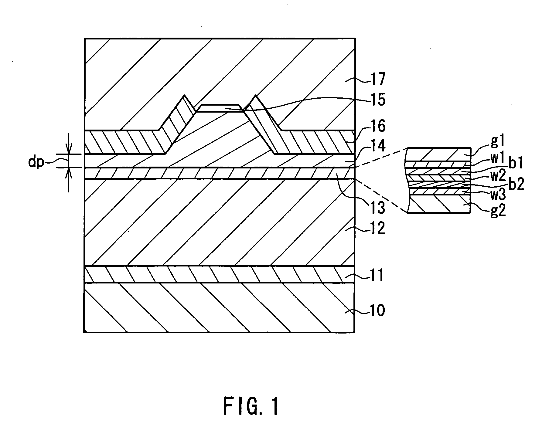
[0038]FIG. 1 is a sectional view showing an example of the semiconductor laser device in the present embodiment. A semiconductor laser device shown in FIG. 1 is formed on an n-type GaAs substrate 10 having a plane tilted by 10° in a [011] direction from a (100) plane as a principal plane. An n-type GaAs buffer layer 11, an n-type (AlGa)InP first cladding layer 12, an active layer 13, a p-type (AlGa)InP second cladding layer 14 and a p-type GaInP protective layer 15 are stacked in this order on the n-type GaAs substrate 10. In this way, a double hetero structure in which the active layer 13 is sandwiched by two cladding layers 12 and 14 is formed.

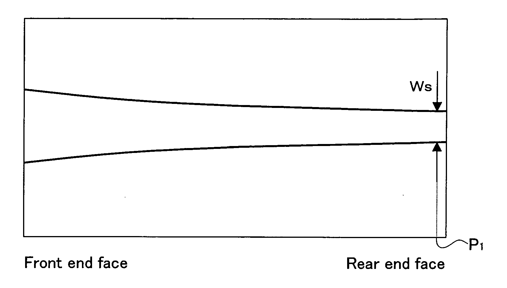
[0039] Furthermore, the p-type (AlGa)InP second cladding layer 14 forms a ridge having a regular mesa shape on the active layer 13. Moreover, an n-type AlInP c...

second embodiment

[0069] An optical pickup apparatus in the second embodiment will be described with reference to FIGS. 8 and 9. The optical pickup apparatus of the present embodiment includes the semiconductor laser device in the above-described embodiment and a photodetector portion for receiving light that is emitted from the semiconductor laser device and then reflected by a recording medium.

[0070]FIG. 8 is a sectional view showing an example of the optical pickup apparatus in the present embodiment. This optical pickup apparatus has a configuration in which a semiconductor laser device 20 is placed on a supporting substrate 21 and a photodetector element 22 is formed on the supporting substrate 21. The supporting substrate 21 has a step portion, and the semiconductor laser device 20 is fixed to a lower surface of this supporting substrate 21 via a base 23. An optical element 24 is formed on an inclined surface of the step portion. The photodetector element 22 is formed on a higher surface of th...


PUM

PropertyMeasurementUnit
widthaaaaaaaaaa
wavelength bandaaaaaaaaaa
reflectivityaaaaaaaaaa

Abstract

A semiconductor laser device has a striped structure for injecting carriers and includes a first electrically-conductive cladding layer, an active layer, and a second electrically-conductive cladding layer that are formed on a substrate. A width of the stripe changes along a resonator direction, a difference between L1 and Lt is within 200 μm, and Rf<Rr, where L1 is a distance from a front end face to a position at which the width of the stripe is minimal, L is a length of a resonator of the semiconductor laser device, Rf is a reflectivity of the front end face, Rr is a reflectivity of a rear end face, and Lt is a distance expressed by L×Loge(Rf) / Loge(Rf×Rr). The saturation of a light emission efficiency is suppressed in a high power operation, allowing a stable fundamental transverse mode oscillation.

Description

BACKGROUND OF THE INVENTION [0001] 1. Field of the Invention [0002] The present invention relates to a semiconductor laser device in which the saturation of a light emission efficiency in a high power operation is suppressed, and an optical pickup apparatus using the same. [0003] 2. Description of Related Art [0004] A semiconductor laser device (in the following, also referred to as a semiconductor laser) is in wide use in various fields. For example, since an AlGaInP semiconductor laser emits red laser light in a wavelength band of 650 nm, it is used widely as a light source in the field of optical disk systems such as DVDs. As an exemplary structure of the semiconductor laser, a double hetero structure including an active layer and two cladding layers sandwiching the active layer, in which one of the cladding layers forms a mesa-shaped ridge is known (see JP 2001-196694 A, for example). [0005]FIG. 10 shows an example of an AlGaInP semiconductor laser having such a structure. The c...

Claims


Application Information

Patent Timeline
Patent Type & Authority Applications(United States)
IPC IPC(8): G11B7/125G11B7/12G11B7/123G11B7/135H01S5/00H01S5/02H01S5/028H01S5/22H01S5/223H01S5/30H01S5/343
CPCB82Y20/00G11B7/1205H01S5/0071H01S5/02248H01S5/02292H01S5/028H01S5/34326H01S5/101H01S5/1014H01S5/2201H01S5/2206H01S5/2219H01S5/2231H01S5/0655G11B7/123H01S5/02255H01S5/02325F24F7/10F24F7/08F24F13/30F24F13/28F24F2221/17
Inventor TAKAYAMA, TORU
Owner PANASONIC SEMICON SOLUTIONS CO LTD
Why Eureka
Try Eureka