Process for vertically patterning substrates in semiconductor process technology by means of inconformal deposition

Inactive Publication Date: 2005-07-28
POLARIS INNOVATIONS
View PDF5 Cites 51 Cited by
  • Summary
  • Abstract
  • Description
  • Claims
  • Application Information

AI Technical Summary

Benefits of technology

[0010] Therefore, it is an object of the present invention to provide a process which, in a simple way, allows a covering layer of substantially uniform layer thicknes

Problems solved by technology

It is not directly possible to pattern reliefs in a direction which is vertical with respect to the substrate surface by means of photolithographic methods.
However, in this process it is difficult to control the way in which the layers produced end in the depth direction.
Furthermore, layers of this type have very considerable differences in thickness bet

Method used


Image

  • Process for vertically patterning substrates in semiconductor process technology by means of inconformal deposition
  • Process for vertically patterning substrates in semiconductor process technology by means of inconformal deposition
  • Process for vertically patterning substrates in semiconductor process technology by means of inconformal deposition

Examples


Example

EXAMPLE 1

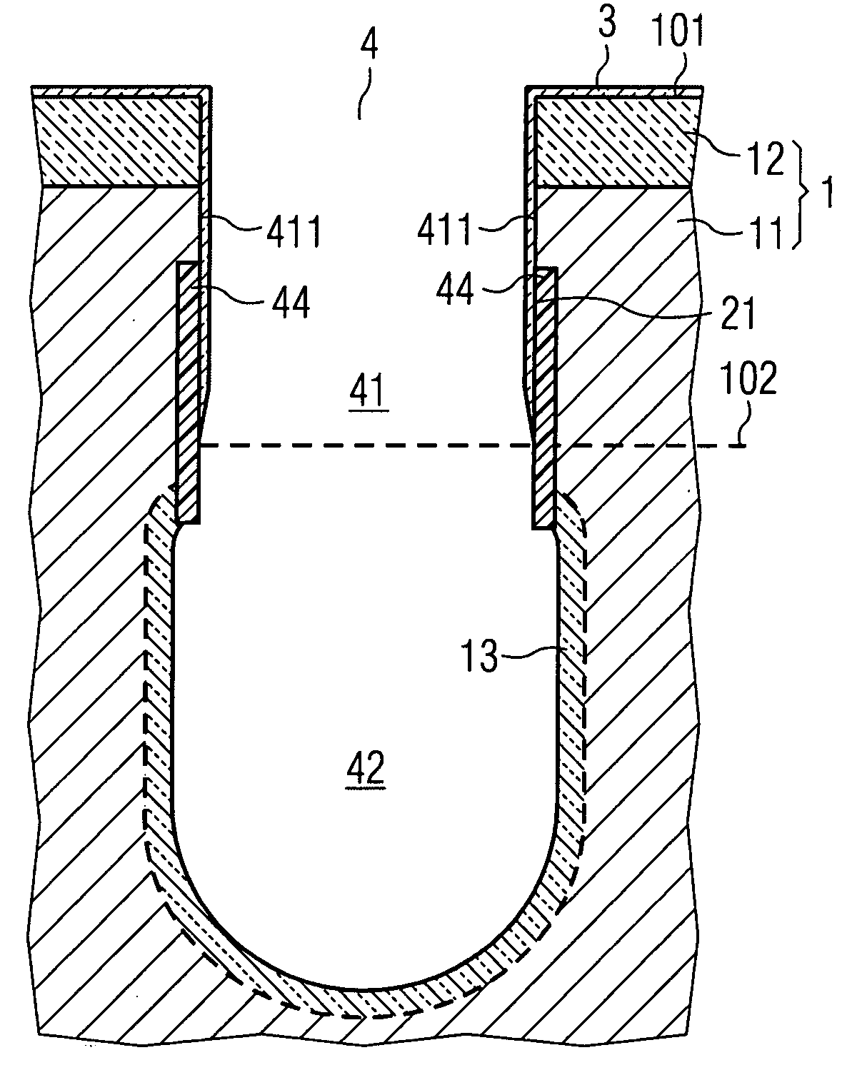
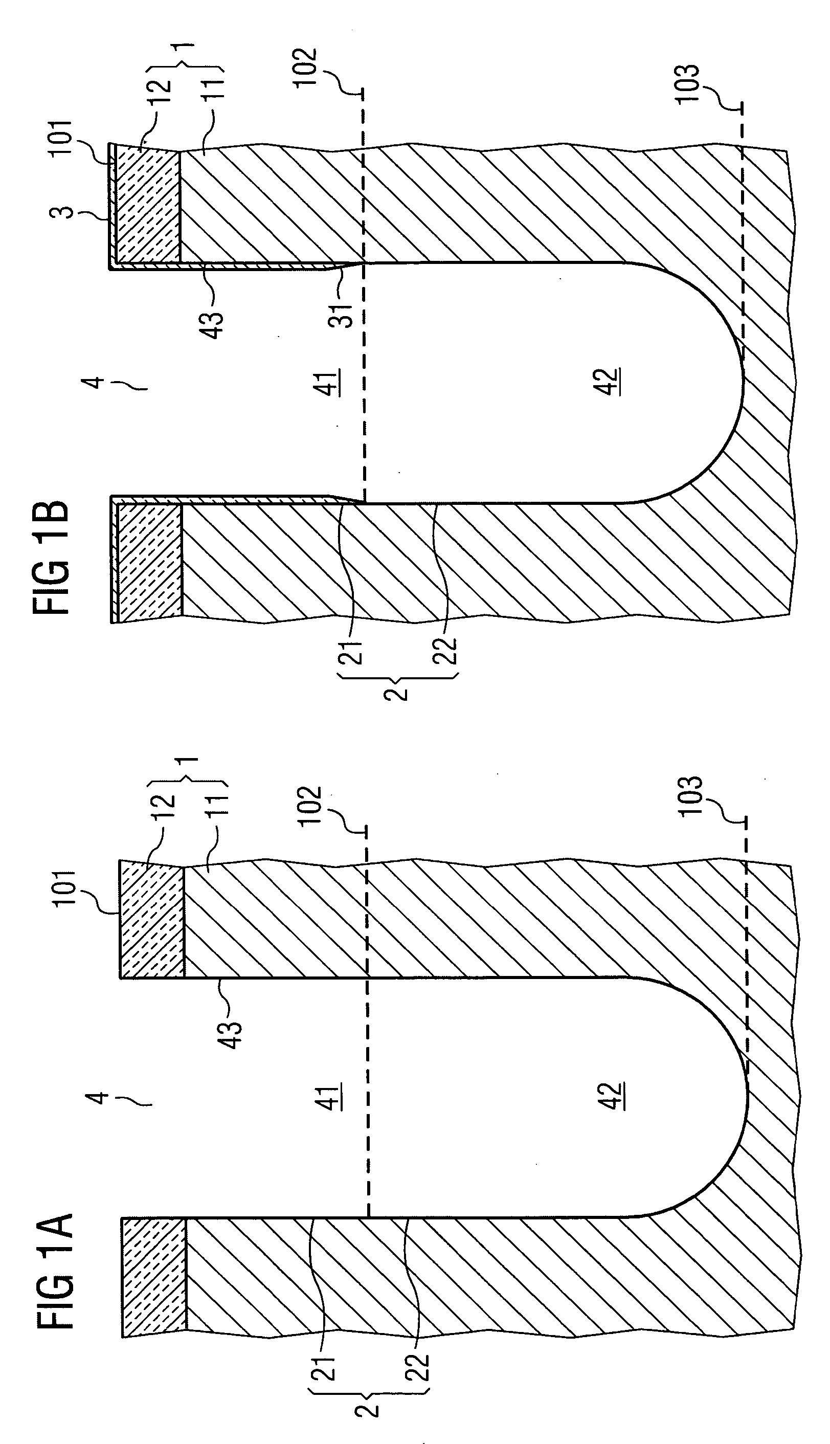
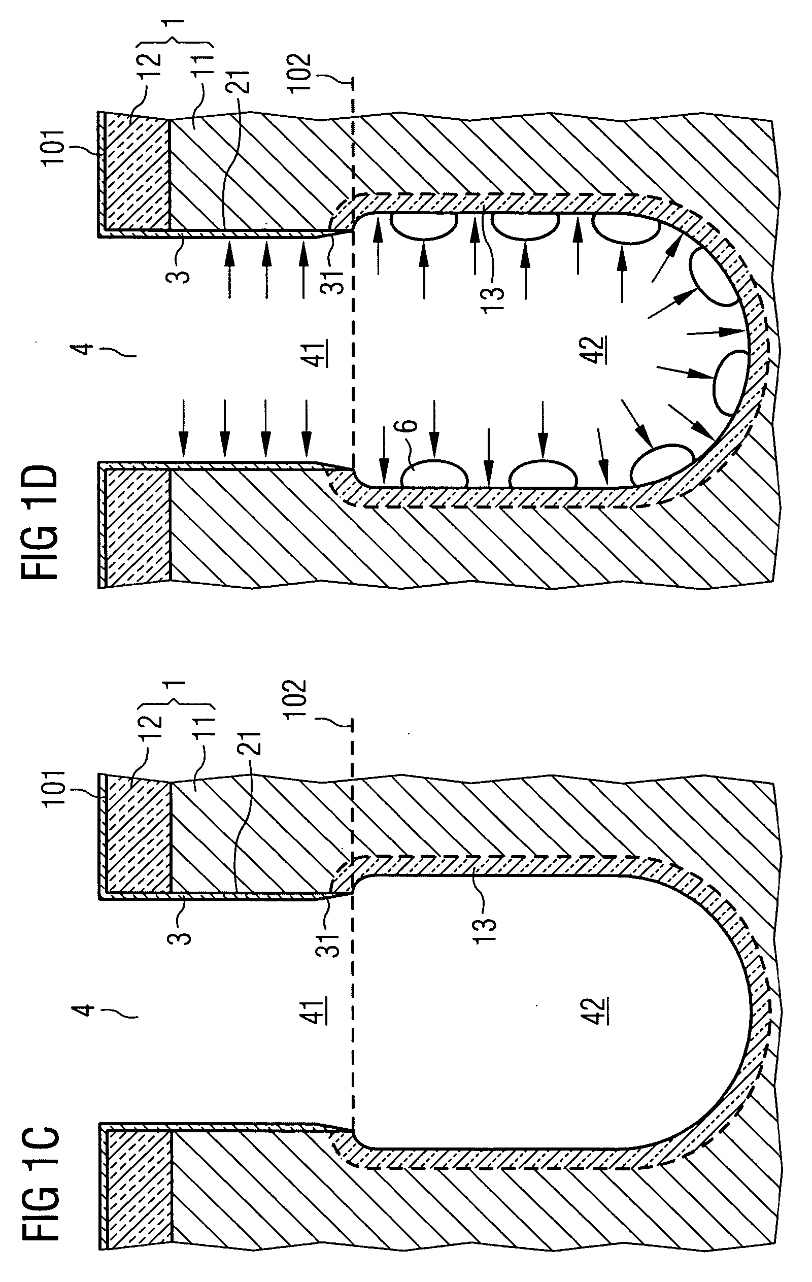
[0082] During the processing of vertical transistor structures, such as trench power transistors and IGBTs (isolated gate bipolar transistors), the doping of a drain zone is advantageously simplified by a covering layer which is deposited inconformally in accordance with the invention and acts as a doping barrier. For this purpose, trenches, in each of which a gate electrode will be provided in the subsequent process sequence, are first introduced into a substrate. In an upper region, which in the finished structure lies opposite source and channel zones formed in the substrate, the trenches are lined with a doping barrier which has been deposited inconformally in accordance with the invention. Then, the drain zone, adjacent to a lower region of the trenches, of the substrate is doped and then the doping barrier is removed.

Example

EXAMPLE 2

[0083] An increasing integration density in integrated circuits means that it is necessary, during the processing of these circuits, to provide through-contacts leading to structures in a deep layer arranged beneath an upper layer, from a substrate surface through an upper layer with conductive regions which have already been formed. The conductive regions are in this case doped semiconductor regions or metallizations. For this purpose, an opening (channel) is etched into the substrate as far as the lower layer and is then filled with a conductive material.

[0084] If, on account of manufacturing tolerances during the formation of the openings, sections of the conductive regions of the upper layer are uncovered by an opening and then the opening is filled with a conductive material, the result is a generally unintended electrical connection between the conductive regions of the upper layer and the deep layer.

[0085] Now, in accordance with the invention, after the openings ...


PUM

PropertyMeasurementUnit
Pressureaaaaaaaaaa
Concentrationaaaaaaaaaa
Electrical resistanceaaaaaaaaaa

Abstract

On a substrate surface, which has been patterned in the form of a relief, of a substrate, typically of a semiconductor wafer, a deposition process is used to provide a covering layer on process surfaces which are vertical or inclined with respect to the substrate surface. The covering layer is patterned in a direction which is vertical with respect to the substrate surface by limiting a process quantity of at least one precursor material and/or by temporarily limiting the deposition process, and is formed as a functional layer or mask for subsequent process steps.

Description

CROSS REFERENCE TO RELATED APPLICATIONS [0001] This application is a continuation of PCT / DE03 / 02438, filed Jul. 21, 2003, and titled “Method for the Vertical Structuring of Substrates in Semiconductor Process Technology by Means of Non-Conforming Deposition,” which claims priority under 35 U.S.C. §119 to German Application No. DE 102 34 735.2, filed on Jul. 30, 2002, and titled “Method for the Vertical Structuring of Substrates in Semiconductor Process Technology by Means of Non-Conforming Deposition,” the entire contents of which are hereby incorporated by reference.FIELD OF THE INVENTION [0002] The invention relates to a process for patterning process surfaces of a substrate that includes a relief, where the surfaces are vertical and / or inclined with respect to a horizontal substrate surface and extend down to a relief depth with respect to the substrate surface, and where a coverage depth is predetermined between the relief depth and the substrate surface. BACKGROUND [0003] In se...

Claims


Application Information

Patent Timeline
IPC IPC(8): C23C16/04C23C16/44C23C16/455H01L21/285H01L21/3065H01L21/314H01L21/334H01L21/768H01L21/8242H01L27/108H01L29/94
CPCC23C16/045C23C16/45525H01L21/28562H01L21/3065H01L21/3141H01L29/945H01L27/10808H01L27/10829H01L27/10852H01L27/1087H01L29/66181H01L21/76879H01L21/02186H01L21/0228H01L21/0217H01L21/02304H01L21/02192H01L21/02164H01L21/02189H01L21/02205H01L21/02214H01L21/02178H01L21/02181H10B12/31H10B12/37H10B12/0387H10B12/033H10B99/00H10B12/00
Inventor HECHT, THOMASGOLDBACH, MATTHIASSCHRODER, UWE
Owner POLARIS INNOVATIONS
Why Eureka
Try Eureka