Method for fabricating semiconductor device and apparatus for fabricating the same

a semiconductor device and apparatus technology, applied in the field of methods, can solve the problems of low productivity of conventional fsa techniques, and achieve the effect of convenient and reliable mounting

Inactive Publication Date: 2005-07-28
PANASONIC CORP
View PDF6 Cites 38 Cited by
  • Summary
  • Abstract
  • Description
  • Claims
  • Application Information

AI Technical Summary

Benefits of technology

[0007] An object of the present invention is that the conventional problem mentioned above is overcome and in a semiconductor device in which a plurality of semiconductor elements (chips) are mounted onto a substrate, the semiconductor chips can be easily and reliably mounted even by using a FSA technique, i.e., by pouring a suspension including the semiconductor chips spread therein over the surface of the substrate.

Problems solved by technology

However, these conventional FSA techniques have the disadvantage of very low productivity, because the function blocks fall and are disposed into the recessed portions in the substrate randomly, and in order to make all of the recessed portions formed in the substrate have the function blocks therein, the function blocks have to be spread in large quantities over the surface of the substrate.

Method used


Image

  • Method for fabricating semiconductor device and apparatus for fabricating the same
  • Method for fabricating semiconductor device and apparatus for fabricating the same
  • Method for fabricating semiconductor device and apparatus for fabricating the same

Examples


first embodiment

[0054] Hereinafter, a first embodiment of the present invention will be described with reference to the accompanying drawings.

[0055]FIG. 1 schematically illustrates a cross sectional configuration of a semiconductor-device fabrication apparatus according to the first embodiment of the present invention.

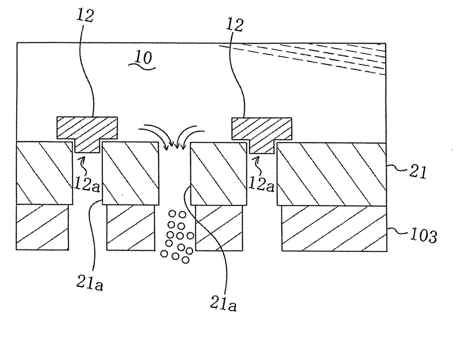
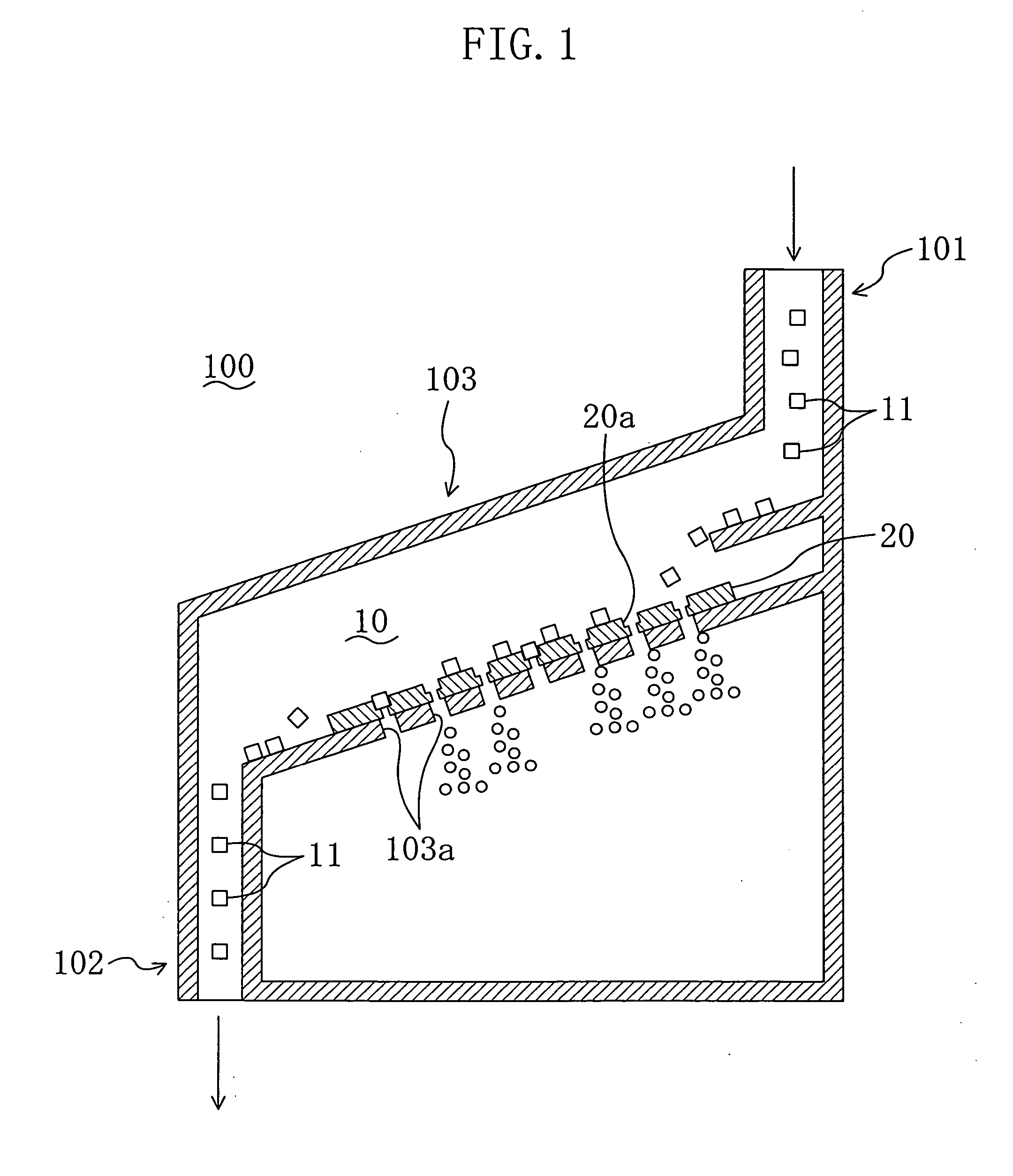
[0056] As shown in FIG. 1, a semiconductor-device fabrication apparatus 100, in which a FSA technique is used, includes a block disposition portion 103 having an inlet portion 101 and an outlet portion 102 at its upper and lower ends, respectively. From the inlet portion 101, a liquid 10 in the form of slurry, in which a plurality of semiconductor elements 11 in the form of chips (hereinafter referred to as “function blocks”) have been spread, is supplied, and the liquid 10 supplied is discharged from the outlet portion 102.

[0057] The bottom face and upper face of the block disposition portion 103 are formed to be inclined with respect to the horizontal surface so that the liquid 1...

second embodiment

[0070] Hereinafter, a second embodiment of the present invention will be described with reference to the accompanying drawings.

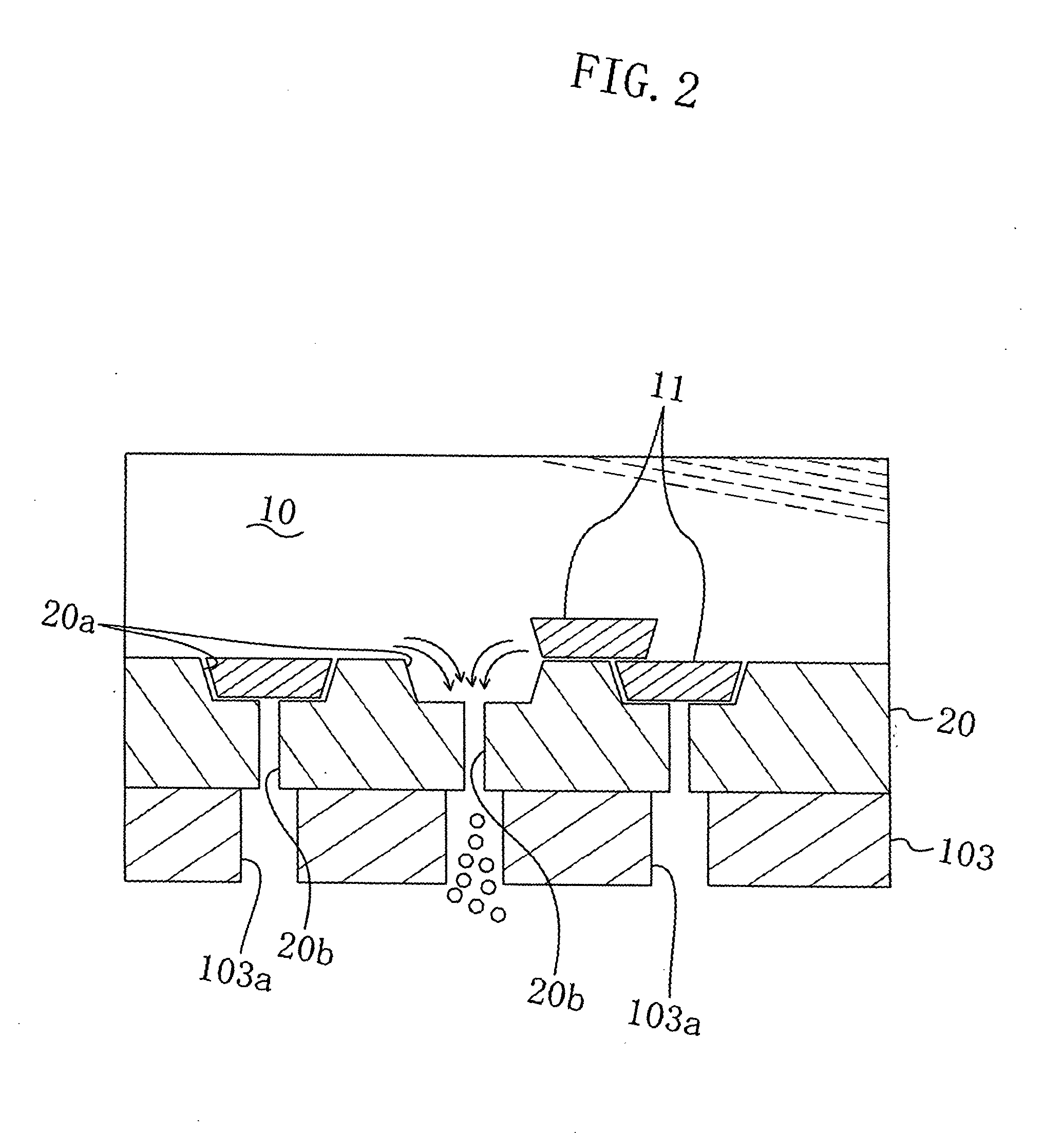
[0071]FIG. 5 schematically illustrates a cross sectional configuration of a semiconductor-device fabrication apparatus according to the second embodiment of the present invention. FIG. 6 shows in enlarged scale a block disposition portion and a substrate held thereon. In FIGS. 5 and 6, the same members as those shown in FIGS. 1 and 2 are identified by the same reference numerals and the description thereof will be omitted herein.

[0072] As shown in FIGS. 5 and 6, the semiconductor-device fabrication apparatus 100 of the second embodiment includes a plurality of pipes 104 connected to individual openings 103a formed in the block disposition portion 103. The pipes 104 are connected at their respective lower ends to a collection pipe 105 for gathering together a liquid 10 flowing through the respective pipes 104. The liquid 10 gathered in the collection pipe 1...

third embodiment

[0077] Hereinafter, a third embodiment of the present invention will be described with reference to the accompanying drawings.

[0078]FIG. 8 shows in enlarged scale a block disposition portion and a substrate held thereon in a semiconductor-device fabrication apparatus according to the third embodiment of the present invention. In FIG. 8, the same members as those shown in FIG. 6 are identified by the same reference numerals and the description thereof will be omitted herein.

[0079] As shown in FIG. 8, in the semiconductor-device fabrication apparatus of the third embodiment, magnetic valves 106 are interposed in pipes 104 formed under openings 103a of a block disposition portion 103. The magnetic valves 106 can be selectively opened or closed from outside the apparatus.

[0080] In the third embodiment, when the magnetic valves 106 are opened, a liquid 10 flows externally from the block disposition portion 103 through through holes 20b formed in a substrate 20 and through the openings...


PUM


Abstract

In a semiconductor-device fabrication method, a plurality of recessed portions are first formed in the principal surface of a substrate. Then, a through hole, passing through the substrate in the front-to-back direction of the substrate, is formed under a portion of the bottom of each recessed portion in the substrate. Subsequently, a plurality of semiconductor elements in the form of chips are spread in a liquid, and the semiconductor-element-spread liquid is poured over the principal surface of the substrate, while passing the liquid through the through holes, so that the semiconductor elements fit into the recessed portions in a self-aligned manner. In this way, the semiconductor elements are disposed into the recessed portions in the substrate in a self-aligned manner.

Description

CROSS-REFERENCE TO RELATED APPLICATION [0001] The disclosure of Japanese Patent Application No. 2004-15849 filed on Jan. 23, 2004 including specification, drawings and claims is incorporated herein by reference in its entity. BACKGROUND OF THE INVENTION [0002] The present invention relates to methods for fabricating semiconductor devices, which enable semiconductor elements to be mounted on a substrate in a self-aligned manner, and also relates to apparatuses for fabricating the semiconductor devices. [0003] In recent years, mounting methods in which a fluidic self-assembly (hereinafter referred to as “FSA”) technique is used have been developed as one type of device-mounting method. [0004] In the FSA technique, devices (hereinafter referred to as “function blocks”), ranging in size from 10 μm to several hundred μm and having given shapes, are spread in a liquid to form a slurry. The liquid (suspension) in the form of slurry is poured over the surface of a substrate made of, e.g., s...

Claims


Application Information

Patent Timeline
Patent Type & Authority Applications(United States)
IPC IPC(8): B65G49/02G01R31/26H01L21/44H01L21/50H01L21/66H01L21/76H01L21/98
CPCH01L24/95H01L25/50H01L2224/95085H01L2224/95136H01L2924/01015H01L2924/01027H01L2924/01033H01L2924/15155H01L2924/15165H01L2924/10158H01L2924/01006H01L2924/15153H01L2924/12042H01L2924/00
Inventor ONOZAWA, KAZUTOSHI
Owner PANASONIC CORP
Why Eureka
Try Eureka