Liquid crystal display device's substrate, liquid crystal display device including the same, and manufacturing method of the same

a technology of liquid crystal display device and substrate, which is applied in non-linear optics, instruments, optics, etc., can solve the problems of poor visual angle characteristics, low transmission factor, and feeling of dark

Active Publication Date: 2005-08-04
SHARP KK
View PDF8 Cites 11 Cited by
  • Summary
  • Abstract
  • Description
  • Claims
  • Application Information

AI Technical Summary

Benefits of technology

[0016] An object of the present invention is to provide a liquid crystal display device in which excellent display characteristics can be obtained, a manufacturing method of the same, and a liquid crystal display device's substrate used for the same.
[0017] Besides, another object of the invention is to provide a liquid crystal display device in which an open area ratio is improved easily and certainly without causing defects such as an uneven display and a highly reliable liquid crystal display is realized, and a manufacturing method of the same.
[0023] Further, the above objects can be achieved by a manufacturing method of a liquid crystal display device comprising a pair of substrates disposed to be opposite to each other, a liquid crystal sealed between the pair of substrates, and a seal member for sealing peripheries of the pair of substrates, and characterized in that at a step of injecting the liquid crystal into a space between the pair of substrates, the liquid crystal is injected into the space between the pair of substrates so that an injection speed of the liquid crystal in a vicinity of the seal member is lower than an injection speed of the liquid crystal in a display region.

Problems solved by technology

This TN mode liquid crystal display device has a problem that its visual angle characteristics are poor, and various studies have been carried out to improve the visual angle characteristics.
Thus, the conventional MVA mode liquid crystal display device has a problem that the transmission factor is low as compared with the TN mode liquid crystal display device and its display causes a feeling of dark.
Its main cause is that portions above the alignment regulating structures become the boundaries of alignment division to generate dark lines, and the transmission factor becomes low.
However, in that case, since the alignment regulating structures becomes few in number, even if a predetermined voltage is applied to a liquid crystal, it takes a long time for the alignment to become stable, and the response speed becomes low.
Further, it can not be neglected that the formation itself of the minute and fine projections or slits complicates the manufacturing process and increases the manufacturing cost.
Thus, a rubbing treatment of an alignment film becomes unnecessary.
This phenomenon indicates that a different color is reproduced in not only in achromatic color but also in chromatic color, and there occurs a problem that a desired display image can not be obtained.
However, the manufacture in which the cell gap is controlled for each pixel has a problem that the process becomes complicated and the manufacturing cost is increased.
However, the scaler IC including a frame memory is expensive and lacks versatility.

Method used


Image

  • Liquid crystal display device's substrate, liquid crystal display device including the same, and manufacturing method of the same
  • Liquid crystal display device's substrate, liquid crystal display device including the same, and manufacturing method of the same
  • Liquid crystal display device's substrate, liquid crystal display device including the same, and manufacturing method of the same

Examples


first embodiment

[0068] A liquid crystal display device according to a first embodiment of the invention, a manufacturing method of the same, and a liquid crystal display device's substrate used for the same will be described by using examples.

example 1-1

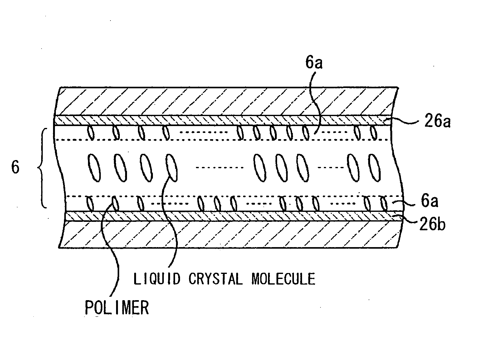
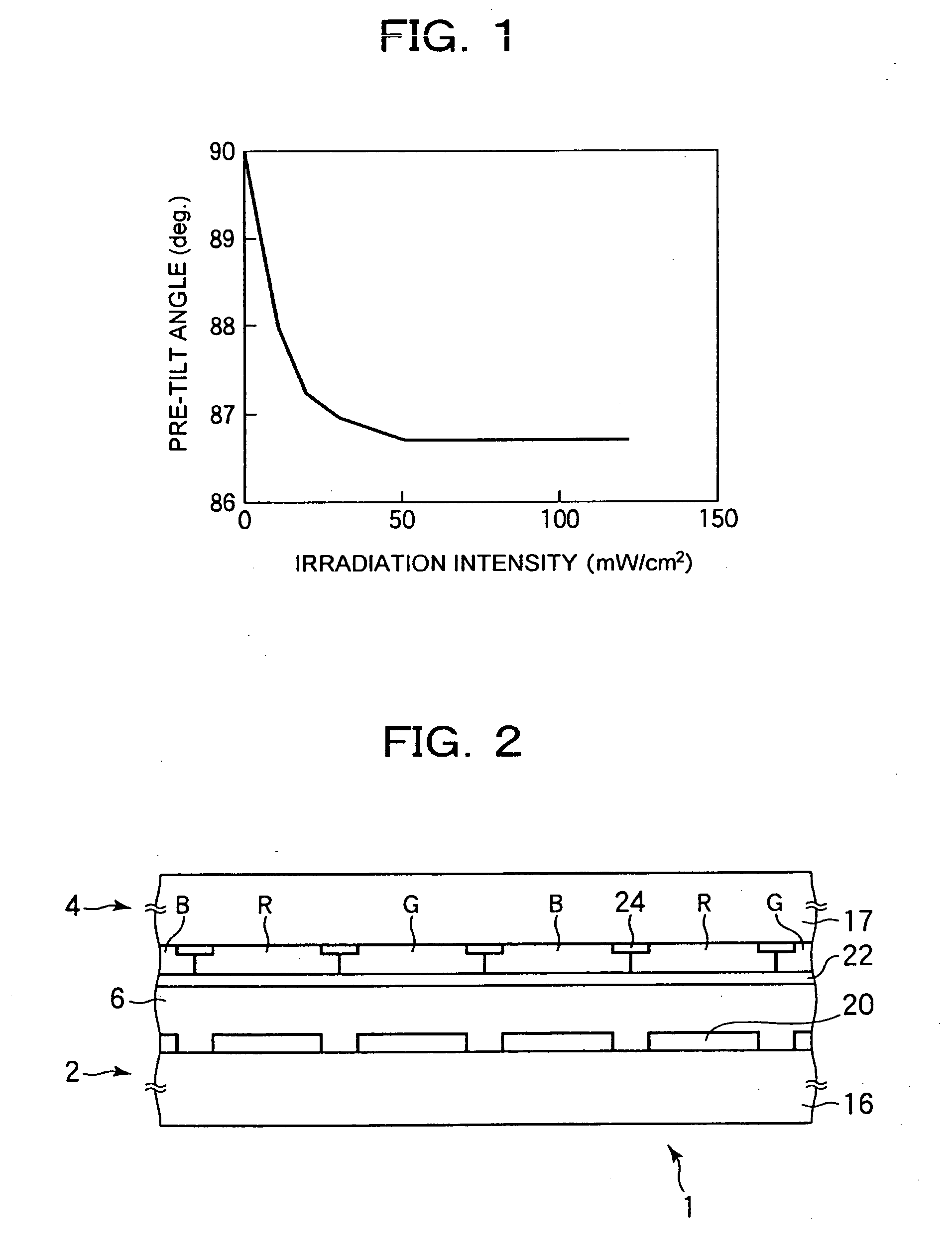
[0069] First, a liquid crystal display device according to example 1-1 of this embodiment and a manufacturing method thereof will be described with reference to FIGS. 1 to 3. In this example, when a polymer for regulating the alignment of a liquid crystal molecule at the time of driving is formed, the irradiation intensity of UV light to be irradiated is made different for each region, so that the same pre-tilt angle is given to a liquid crystal layer in the whole display region. By this, uniform T-V characteristics can be obtained in the whole display region.

[0070] The principle of the manufacturing method of the liquid crystal display device according to this example will be described. FIG. 1 is a graph showing the relation between the irradiation intensity of UV light and the pre-tilt angle of a liquid crystal molecule. The horizontal axis indicates the irradiation intensity (mW / cm2) of the UV light, and the vertical axis indicates the pre-tilt angle (deg.) of the liquid crystal...

example 1-2

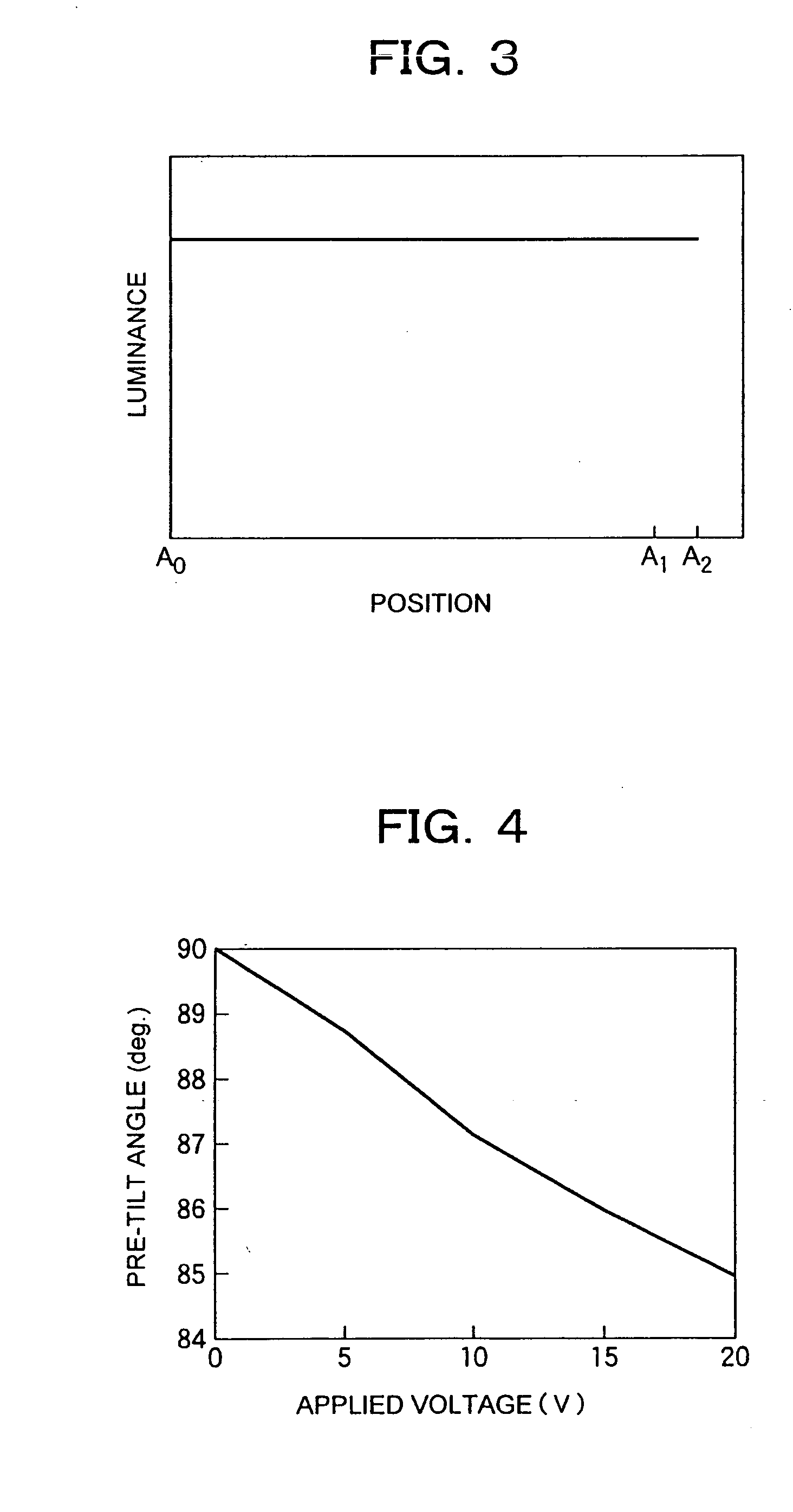
[0078] Next, a manufacturing method of a liquid crystal display device according to example 1-2 of this embodiment will be described with reference to FIG. 4. In this example, in order to give different pre-tilt angles to liquid crystal molecules of a pixel in which a CF resin layer of R is formed (hereinafter referred to as an R pixel), a pixel in which a CF resin layer of G is formed (hereinafter referred to as a G pixel), and a pixel in which a CF resin layer of B is formed (hereinafter referred to as a B pixel), different voltages are applied to the liquid crystal layer 6 for the respective colors when UV light is irradiated to polymerize a monomer.

[0079]FIG. 4 is a graph showing the relation between the applied voltage and the pre-tilt angle of a liquid crystal molecule. The horizontal axis indicates the applied voltage (V) to the liquid crystal layer 6, and the vertical axis indicates the pre-tilt angle (deg.) of the liquid crystal molecule obtained after the irradiation of a...


PUM

PropertyMeasurementUnit
pre-tilt angleaaaaaaaaaa
voltageaaaaaaaaaa
timeaaaaaaaaaa

Abstract

The invention relates to a manufacturing method of a liquid crystal display device in which an alignment direction of a liquid crystal molecule at the time of driving is regulated by using a polymer, and has an object to provide a manufacturing method of a liquid crystal display device in which excellent display characteristics can be obtained. A liquid crystal layer containing a polymerizable component capable of being polymerized by light is sealed between two substrates arranged to be opposite to each other, the polymerizable component is polymerized by irradiation of light under a predetermined light irradiation condition while a voltage is applied to the liquid crystal layer under a predetermined voltage application condition, and when a pre-tilt angle of a liquid crystal molecule and / or an alignment direction at a time of driving is regulated, at least one of the voltage application condition and the light irradiation condition is changed for each region.

Description

BACKGROUND OF THE INVENTION [0001] 1. Field of the Invention [0002] The present invention relates to a liquid crystal display device for regulating the alignment direction of a liquid crystal molecule at the time of driving by using a polymer, a manufacturing method of the same, and a liquid crystal display device's substrate used for the same. [0003] Besides, the invention relates to a liquid crystal display device and a manufacturing method of the same, and particularly to a liquid crystal display device in which an uneven display can be reduced and a manufacturing method of the same. [0004] 2. Description of the Related Art [0005] Conventionally, as an active matrix type liquid crystal display device, a twisted nematic (TN) mode is widely used in which a liquid crystal material having a positive dielectric anisotropy is aligned to be horizontal with respect to a substrate surface in a dark state and to be twisted 90 degrees between opposite substrates. [0006] This TN mode liquid ...

Claims


Application Information

Patent Timeline
Patent Type & Authority Applications(United States)
IPC IPC(8): G02F1/1333G02F1/1337G02F1/1341G02F1/139
CPCG02F1/133707G02F1/133753G02F1/1393G02F1/1341G02F1/133788G02F1/13
Inventor KISHIDA, KATSUHIKONAKANISHI, YOHEITSUDA, HIDEAKIHANAOKA, KAZUTAKAINOUE, YUICHISHIBASAKI, MASAKAZU
Owner SHARP KK
Why Eureka
Try Eureka