Method for analyzing defect data and inspection apparatus and review system

a technology of defect data and inspection apparatus, applied in the direction of image enhancement, semiconductor/solid-state device testing/measurement, instruments, etc., can solve the problems of large amount of data to be accumulated, cannot be used for distribution, and cannot be recognized as a cluster, etc., to achieve the effect of easy identification of the cause of defects in the apparatus or process

Inactive Publication Date: 2005-08-04
HITACHI LTD +1
View PDF4 Cites 28 Cited by
  • Summary
  • Abstract
  • Description
  • Claims
  • Application Information

AI Technical Summary

Benefits of technology

[0006] It is another object of the invention to provide a defect data analyzing method capable of fast classifying clusters of high-density regions of detected defects at a practical level.
[0008] In addition, according to the method described in the above JP-A-6-61314, patterns of an indeterminate form are registered because known patterns to be used for comparison are produced on the basis of actual wafers. The method in the U.S. Pat. No. 5,982,920 makes clusters of various forms of lines or of indeterminate forms be classified mixed as one type. In either case, when the cause of defect is specified by manpower, skill is required. For automatic inspection, an enormous amount of data must be accumulated, and as a result the computation time increases. Therefore, information that makes the defect cause identification by manpower easy is required to be fast produced.
[0010] According to the invention, since a high-density region image representing a high-density portion of defects is generated on the basis of the position coordinates of defects detected by an inspection apparatus, the high-density region is not required to recognize as cluster, and a relatively high-density region can be extracted even if the distribution is thin. Moreover, according to the invention, since the high-density region image is classified into any one of a plurality of previously registered geometric patterns, the defect distribution states can be analyzed at a practical level in both computing time and storage capacity. Since meaning can be previously created in each of the plurality of geometric patterns, the cause of defect in apparatus or process can be identified with ease.

Problems solved by technology

Therefore, it cannot be used for the distribution that is so thin that the cluster cannot be recognized.
For automatic inspection, an enormous amount of data must be accumulated, and as a result the computation time increases.

Method used


Image

  • Method for analyzing defect data and inspection apparatus and review system
  • Method for analyzing defect data and inspection apparatus and review system
  • Method for analyzing defect data and inspection apparatus and review system

Examples


first embodiment

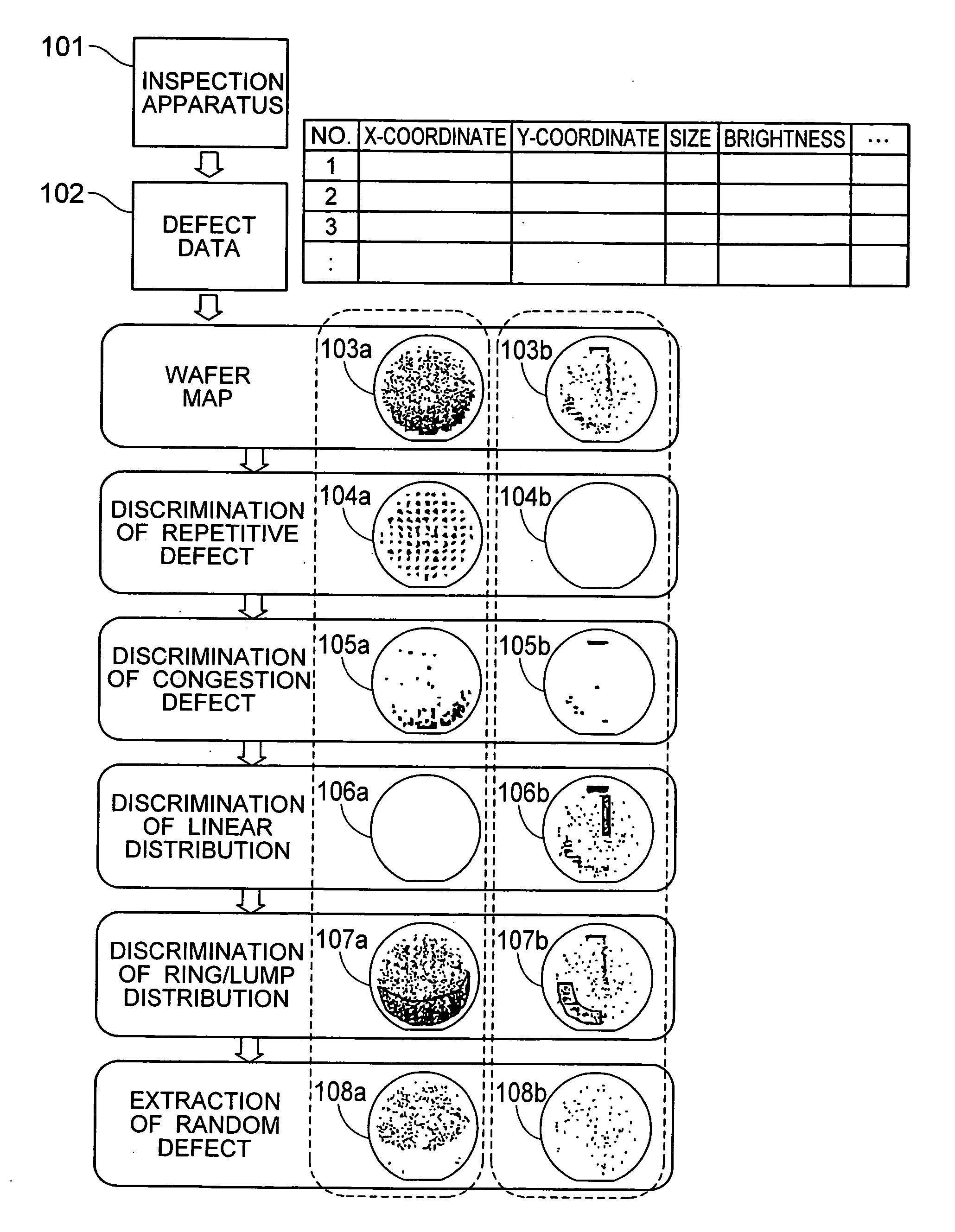
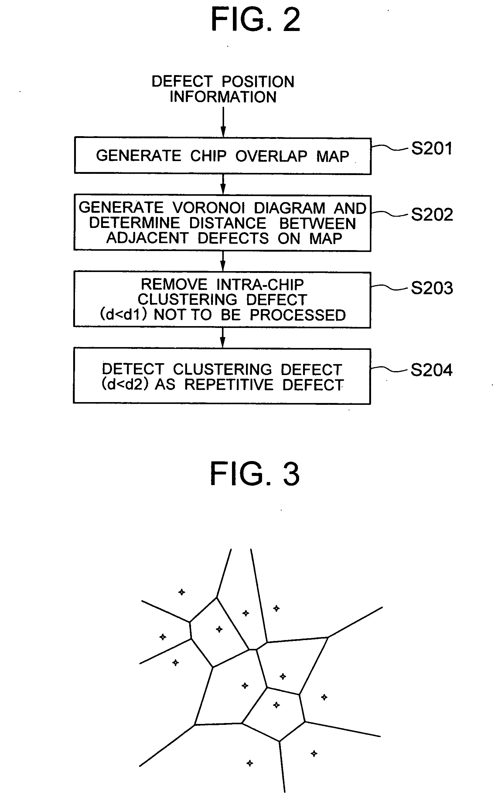
[0032] In the defect data analyzing method according to the invention, defect data 102 produced from a semiconductor substrate inspection apparatus 101 includes at least the coordinates of defect position. Shown at 103a, 103b are wafer maps for showing the positions of defects expressed by a coordinate system with its origin selected as one point from the wafer. The coordinates of defect that the inspection apparatus produces can be expressed by a coordinate system with its origin selected as one point from the wafer or by coordinate systems with their origins selected from the respective chips of the wafer. In the former case, the coordinate values X, Y of defect are used as they are, but in the latter case it is necessary that the coordinates of defect within a chip be converted to be on another coordinate system by using chip arrangement information and chip size information. The defects on the wafer map are respectively classified on the basis of its defect distribution into dis...

second embodiment

[0075]FIG. 16 shows the construction of the inspection apparatus according to the invention.

[0076] The pattern information adding means 301 adds sampling condition number in addition to the above information. It manually groups the dictionary patterns using the same sampling condition, and attaches the same sampling number. When there is no sampling condition corresponding to the number, sampling condition generation means 307 generates the sampling condition.

[0077] The sampling condition generation means 307 generates the sampling condition for determining a defect for review. It manually generates the sampling conditions associated with the patterns of ring / lump distribution defects, and sampling conditions at each of the other distribution feature categories, and makes them be stored as a sampling condition file 312 in the storage means 302. The sampling conditions are, for example, sampling number, sampling rate and sampling method. The values of sampling number and sampling ra...


PUM

PropertyMeasurementUnit
defectaaaaaaaaaa
distanceaaaaaaaaaa
defect densityaaaaaaaaaa

Abstract

The distribution states of defects are analyzed on the basis of the coordinates of defects detected by an inspection apparatus to classify them into a distribution feature category, or any one of repetitive defect, congestion defect, linear distribution defect, ring / lump distribution defect and random defect. In the manufacturing process for semiconductor substrates, defect distribution states are analyzed on the basis of defect data detected by an inspection apparatus, thereby specifying the cause of defect in apparatus or process.

Description

CROSS REFERENCE TO RELATED APPLICATION [0001] This application is a continuation application of U.S. Ser. No. 10 / 119,018, filed Apr. 10, 2002, the contents of which is incorporated herein by reference.BACKGROUND OF THE INVENTION [0002] The present invention relates to a defect data analyzing method for analyzing defect distribution states from the defect data detected by inspection apparatus in a semiconductor device manufacturing process in which circuit patterns are formed on a semiconductor substrate. [0003] In the semiconductor device manufacturing process in which circuit patterns are formed on a semiconductor substrate (hereafter, referred to as semiconductor substrate production process), pattern defect inspection or foreign matter inspection is executed after each process, and the inspection results are analyzed, in order to improve and stabilize the yield. In other words, the operator observes the detected defects on an optical microscope or scanning electron microscope to ...

Claims


Application Information

Patent Timeline
Patent Type & Authority Applications(United States)
IPC IPC(8): G01N21/95H01L21/66G06T7/00
CPCG01N21/956G06T2207/30148G06T7/001G06T7/0006G01N21/9501
Inventor SHIBUYA, HISAETAKAGI, YUJI
Owner HITACHI LTD
Why Eureka
Try Eureka