Vertical-cavity surface-emitting semiconductor laser

a semiconductor laser and vertical cavity technology, applied in semiconductor lasers, laser details, electrical equipment, etc., can solve the problems of device failure, device deformation, device failure, etc., and achieve the effect of preventing device failure, preventing device failure, and preventing device failur

Inactive Publication Date: 2005-08-04
FUJIFILM BUSINESS INNOVATION CORP
View PDF3 Cites 52 Cited by
  • Summary
  • Abstract
  • Description
  • Claims
  • Application Information

AI Technical Summary

Problems solved by technology

If electrostatic discharge (hereinafter simply referred to as ESD) occurs in the device, spike current instantaneously will flow therein and may break down or degrade the device.
The device is thus defective and is no longer capable of operating normally.
This modifies the optical waveguide mode at an optical output lower than the optical output that causes an edge damage, and thus increases the magnitude of current at which an edge damage occurs.
The method of inclining the plane direction of the substrate disclosed in Japanese Laid-Open Patent Application Publication No 5-243666 is directed specifically to measures for electrostatic damage inherent in the edge-emitting laser, and may not be effective to VCSEL.
The protection device disclosed in Japanese Laid-Open Patent Application Publication No. 11-112026 does not improve the electrostatic damage threshold voltage within the light-emitting device.
Thus, the laser apparatus needs an increased number of components and is thus expensive.
However, desired fundamental characteristics of laser will not be obtained by merely increasing the oxide aperture size.

Method used


Image

  • Vertical-cavity surface-emitting semiconductor laser
  • Vertical-cavity surface-emitting semiconductor laser
  • Vertical-cavity surface-emitting semiconductor laser

Examples


first embodiment

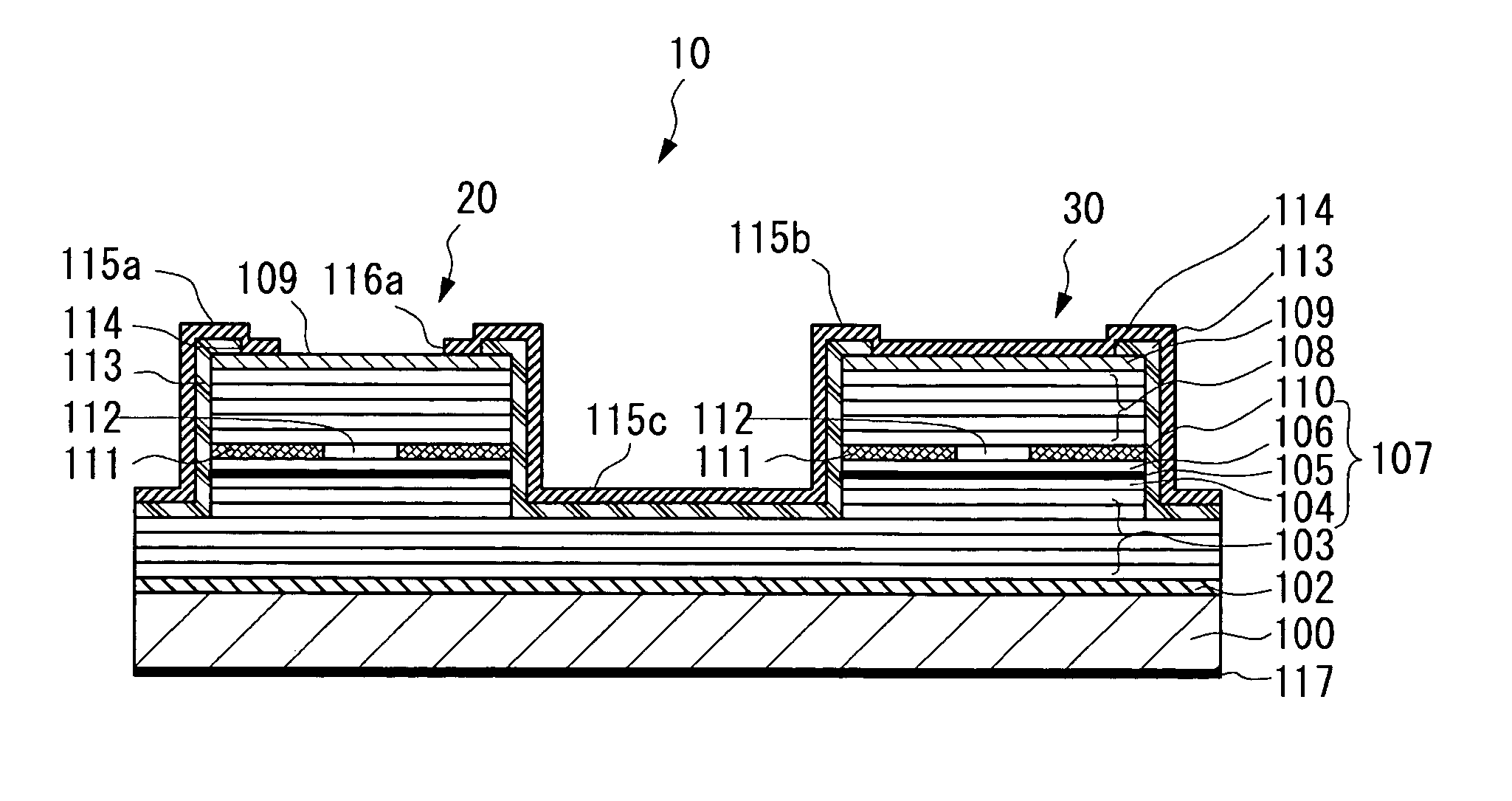
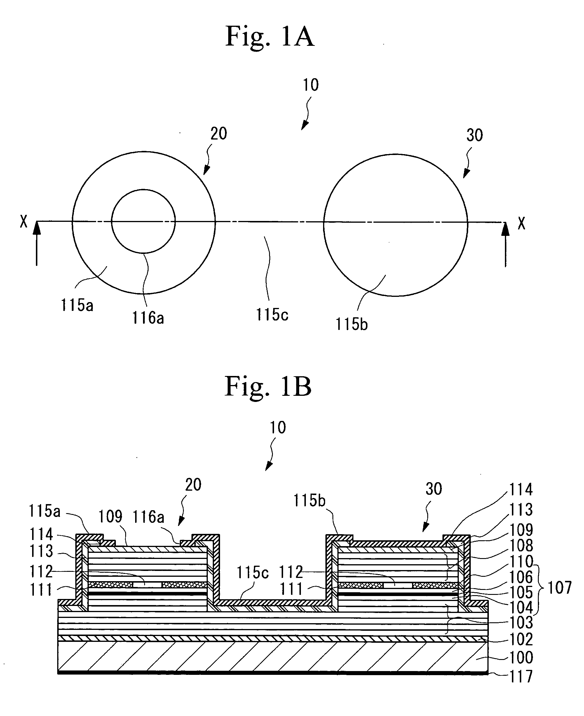
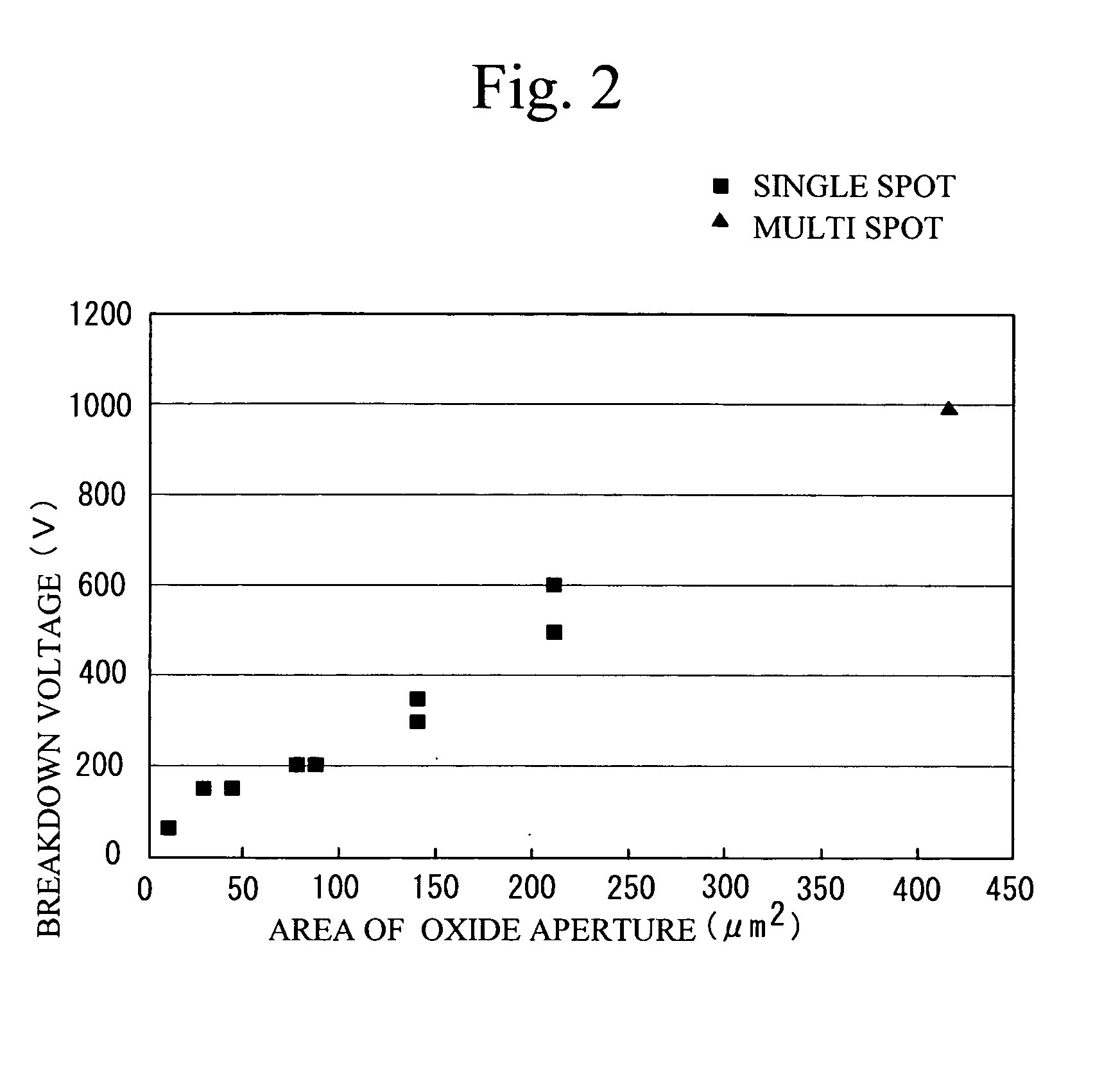
[0021]FIG. 1A is a schematic plan view of a VCSEL according to the present invention, and FIG. 1B is a sectional view taken along a line X-X shown in FIG. 1A. A VCSEL 10 according to the present embodiment has a mesa (first mesa) 20 from which laser light is emitted, and another mesa (second mesa) 30 from which no laser light is emitted. The first and second mesas 20 and 30 are formed on a single substrate. The mesa 30 functions as a dummy that does not emit laser light at all, and substantially increases the area of the oxide aperture of the VCSEL 10. It is therefore possible to improve the ESD-induced damage threshold voltage. The area of the oxide aperture of laser light emitted from the mesa 20 can be reduced to, for example, an area for the single mode, so that the fundamental laser characteristics cannot be degraded at all.

[0022] As shown in FIG. 1B, the VCSEL 10 has an n-type GaAs substrate 100, on which provided are an n-type buffer layer 102, an n-type lower DBR (Distribute...

third embodiment

[0035]FIG. 4A is a plan view of a VCSEL according to the present invention. A VCSEL 14 of the present embodiment has a mesa 24 and four mesas 34. The mesa 24 is located in the center of a substrate 100 and has the function of emitting laser light. The four mesas 34, which are shown by broken lines, are arranged in the vicinity of the mesa 24 so as to surround the mesa 24. The mesas 24 and 34 have a cylindrical shape of the same size. The top of the mesa 24 is covered with the p-side metal layer 115a, which has the laser emission aperture 116a. In contrast, the mesas 34 function as current paths, but do not have any laser emission apertures, so that no laser can be emitted from the mesas 34.

[0036] Preferably, the four mesas 34 are arranged on imaginary diagonal lines that pass through the center of the mesa 24, and are positioned at the same distance from the center of the mesa 24. In order to downsize the VCSEL, it is desirable to arrange the mesas 34 as close to the mesa 24 as poss...


PUM


Abstract

A surface-emitting semiconductor laser includes comprising a substrate, a first mesa that is formed on the substrate and includes at least one mesa capable of emitting laser light, and a second mesa that is formed on the substrate and includes at least one mesa restraining emission of laser light.

Description

BACKGROUND OF THE INVENTION [0001] 1. Field of the Invention [0002] The present invention relates to a vertical-cavity surface-emitting semiconductor laser (VCSEL), and more particularly, to improvements in the electrostatic damage threshold voltage thereof. [0003] 2. Description of the Related Art [0004] VCSEL has technical advantages that a threshold current is small, an optical spot of a circular shape can be easily obtained, and an evaluation at a wafer state and two dimensional array of the light source can be achieved. VCSEL has been expected to be used as a light source for optical communication devices and electronic devices. [0005] VCSEL may happen to be exposed to a high voltage such as static electricity at the time of mounting on a printed-circuit board or the like as in the case of other semiconductor devices. If electrostatic discharge (hereinafter simply referred to as ESD) occurs in the device, spike current instantaneously will flow therein and may break down or deg...

Claims


Application Information

Patent Timeline
Patent Type & Authority Applications(United States)
IPC IPC(8): H01S5/00H01S5/042H01S5/183H01S5/30H01S5/343
CPCB82Y20/00H01S5/0425H01S5/18313H01S5/18358H01S2301/166H01S5/305H01S5/3054H01S5/3432H01S5/18394H01S5/04256
Inventor ISHII, RYOJINAKAYAMA, HIDEOKUWATA, YASUAKI
Owner FUJIFILM BUSINESS INNOVATION CORP
Why Eureka
Try Eureka