Wafer dividing method

a dividing method and dividing line technology, applied in the field of dividing lines, can solve the problems of reducing productivity, reducing productivity, and not always easy cutting with the above-mentioned cutting blades

Active Publication Date: 2005-08-04
DISCO CORP
View PDF4 Cites 44 Cited by
  • Summary
  • Abstract
  • Description
  • Claims
  • Application Information

AI Technical Summary

Benefits of technology

[0007] It is an object of the present invention to provide a wafer dividing method capable of establishing a process comprising the steps of forming a deteriorated layer along dividing lines in the inside of a wafer by using a pulse laser beam, dividing the wafer into individual chips along the deteriorated layers and picking up the chips.

Problems solved by technology

Since the cutting blade has a thickness of about 20 μm, the dividing lines for sectioning chips must have a width of about 50 μm and hence, the area ratio of the dividing lines to the wafer is large, thereby reducing productivity.
Further, since a sapphire substrate, silicon carbide substrate and the like have high Mohs hardness, cutting with the above cutting blade is not always easy.
Although a process for dividing the wafer into individual chips by completely cutting it with the above cutting machine and picking up the chips has been established, a production line making use of this technique is not established yet and its development is under way through trial and error because a technique for forming a deteriorated layer along the dividing lines in the inside of the wafer by using a pulse laser beam cannot divide the wafer perfectly.

Method used


Image

  • Wafer dividing method
  • Wafer dividing method
  • Wafer dividing method

Examples


Embodiment Construction

[0046] Preferred embodiments of the present invention will be described in detail hereinunder with reference to the accompanying drawings.

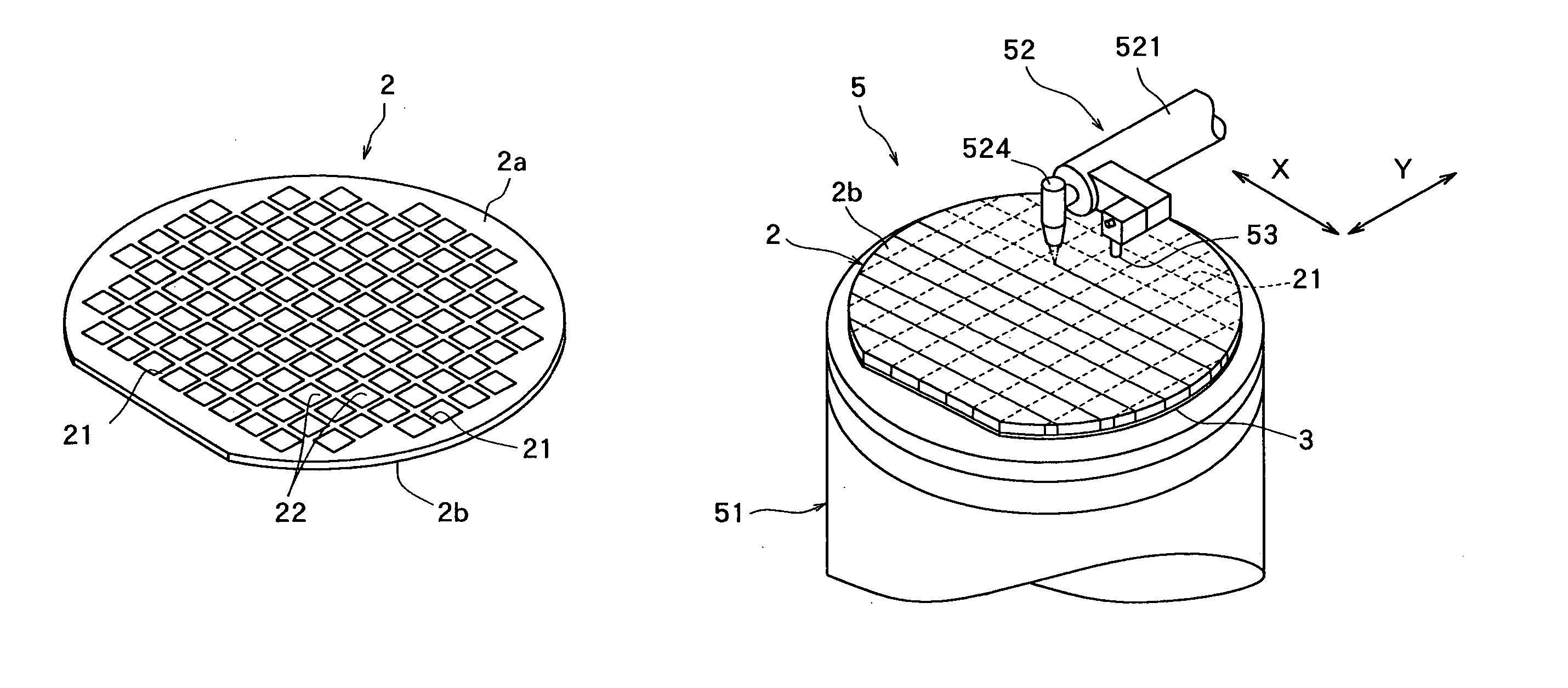
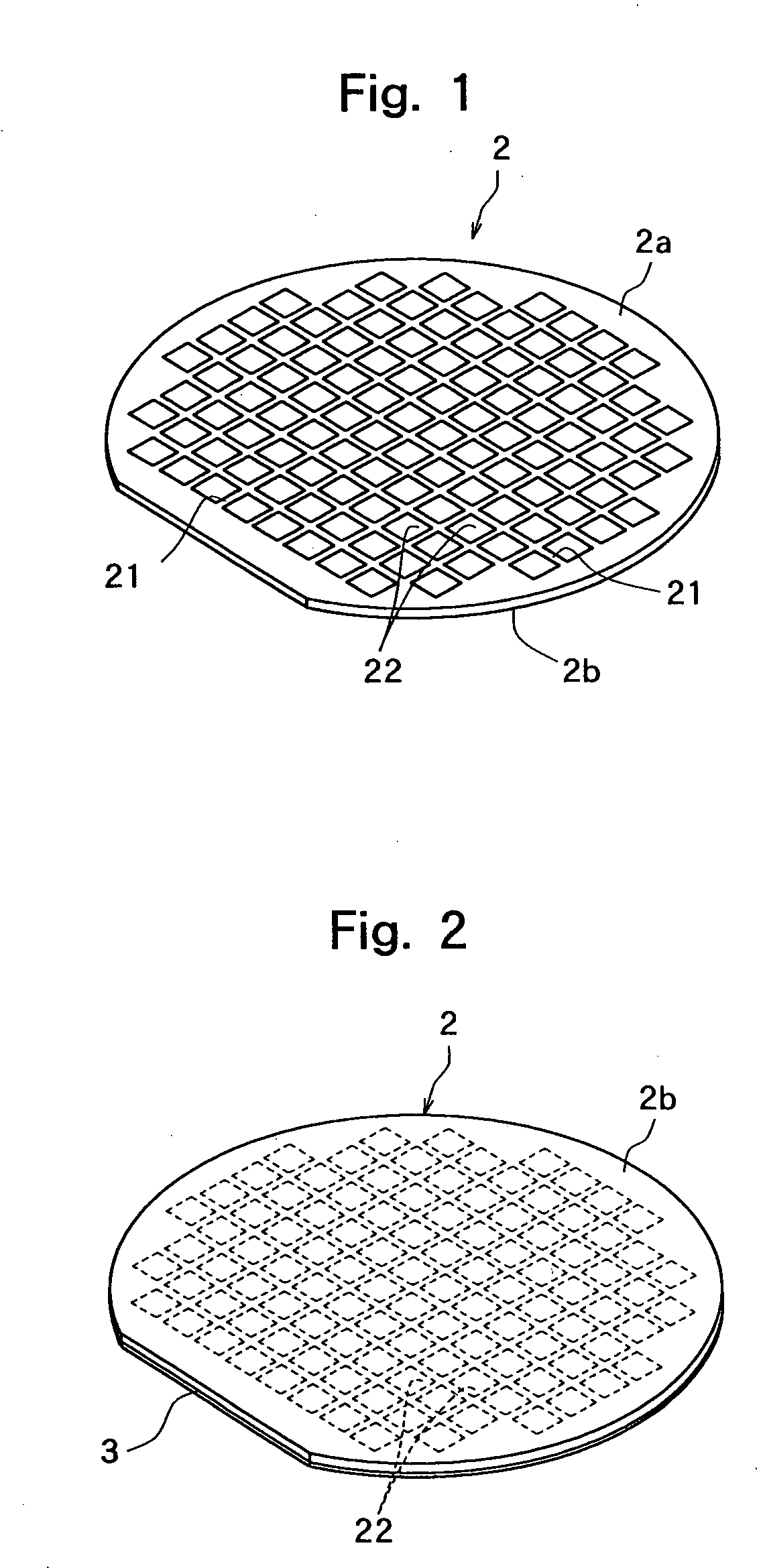
[0047]FIG. 1 is a perspective view of a semiconductor wafer as a wafer to be divided according to the present invention. The semiconductor wafer 2 shown in FIG. 1 is a silicon wafer having a plurality of dividing lines 21 formed in a lattice pattern on the front surface 2a, and circuits 22 are formed as function elements in a plurality of areas sectioned by the plurality of dividing lines 21. A protective member 3 is affixed to the front surface 2a of the thus constituted semiconductor wafer 2, as shown in FIG. 2 (protective member affixing step).

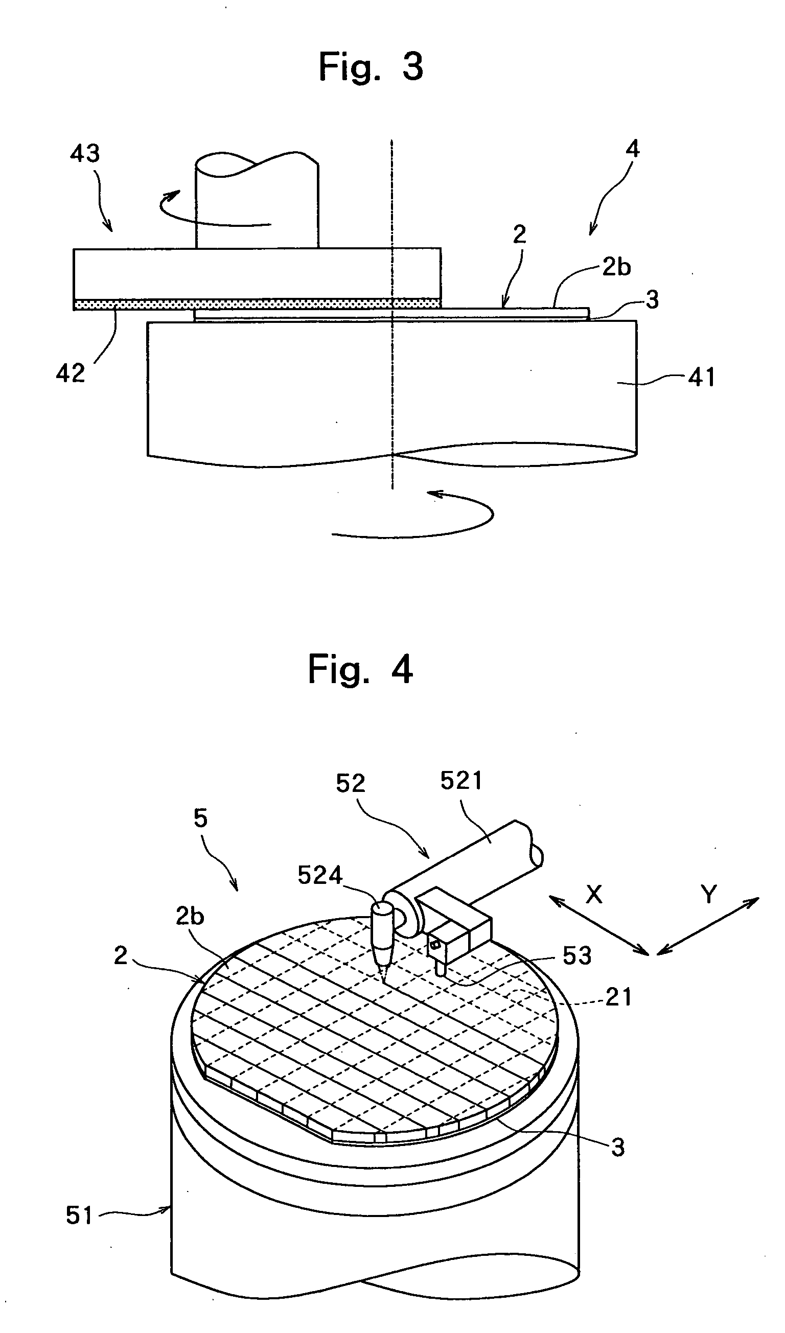
[0048] After the protective member affixing step is carried out to affix the protective member 3 to the front surface 2a of the semiconductor wafer 2, there comes a polish step for polishing the back surface 2b of the semiconductor wafer 2 to make it into a mirror surface. This polishing step is carried...


PUM


Abstract

A method of dividing, along dividing lines, a wafer having function elements formed in areas sectioned by the dividing lines formed in a lattice pattern on the front surface, which comprises: a protective member affixing step for affixing a protective member to the front surface of the wafer; a polishing step for polishing the back surface of the wafer having the protective member affixed to the front surface; a deteriorated layer formation step for forming a deteriorated layer along the dividing lines in the inside of the wafer by applying a pulse laser beam capable of passing through the wafer to the wafer along the dividing lines from the polished back surface side of the wafer; a frame holding step for affixing the back surface of the wafer in which the deteriorated layers have been formed along the dividing lines, to a dicing tape mounted on an annular frame; a dividing step for dividing the wafer into individual chips along the dividing lines by exerting external force along the dividing lines where the deteriorated layers have been formed, of the wafer held on the frame; an expansion step for enlarging the interval between chips by stretching the dicing tape affixed to the wafer divided into individual chips; and a pick up step for picking up the chips from the stretched dicing tape.

Description

FIELD OF THE INVENTION [0001] The present invention relates to a wafer dividing method comprising dividing, along dividing lines, a wafer having function elements formed in areas sectioned by the dividing lines formed in a lattice pattern on the front surface, and picking up the obtained individual chips. DESCRIPTION OF THE PRIOR ART [0002] In the production process of a semiconductor device, a plurality of areas are sectioned by dividing lines called “streets” arranged in a lattice pattern on the front surface of a substantially disk-like semiconductor wafer, and a circuit (function element) such as IC or LSI is formed in each of the sectioned areas. Individual semiconductor chips are manufactured by cutting the semiconductor wafer along the dividing lines to divide it into the areas having a circuit formed therein. An optical device wafer comprising light-sensitive elements (function elements) such as photodiodes or light-emitting elements (function elements) such as laser diodes ...

Claims


Application Information

Patent Timeline
Patent Type & Authority Applications(United States)
IPC IPC(8): H01L21/304H01L21/306H01L21/78
CPCH01L21/3043H01L2221/68336H01L21/78H01L21/30625
Inventor MURATA, MASAHIRONAGAI, YUSUKEMORISHIGE, YUKIOKOBAYASHI, SATOSHIOHMIYA, NAOKI
Owner DISCO CORP
Why Eureka
Try Eureka