Method for manufacturing semiconductor element

a semiconductor element and manufacturing method technology, applied in the direction of manufacturing tools, metal working equipment, welding/soldering/cutting articles, etc., can solve the problems of difficult control of the direction in which the crack runs, the laser beam may sometimes be focused on the outside of the substrate, and the cracks are difficult to control. the effect of accurate splitting along the processed portions

Active Publication Date: 2011-12-08
NICHIA CORP
View PDF2 Cites 37 Cited by
  • Summary
  • Abstract
  • Description
  • Claims
  • Application Information

AI Technical Summary

Benefits of technology

[0025]With laser irradiation, processed portions and a fissure that links adjacent processed portions and runs from the processed portions to the substrate surface are created, which makes possible accurate splitting along the processed portions or fissures. When the laser is directed along the intended dividing...

Problems solved by technology

However, with a method in which a wafer is divided by forming a modification region with a pulsed laser beam only inside of a substrate, the application of external force creates a crack from the modification region inside toward the front and rear faces of the substrate, and this is used to break the wafer, so it is difficult to control the direction in which the crack runs, and the wafer is sometimes divided somewhere other than in the intended division region.
Also, with a method in which grooves are formed by laser irradiation in a substrate surface, the means for forming the separation grooves, which in the past were fo...

Method used


Image

  • Method for manufacturing semiconductor element
  • Method for manufacturing semiconductor element
  • Method for manufacturing semiconductor element

Examples


example 1

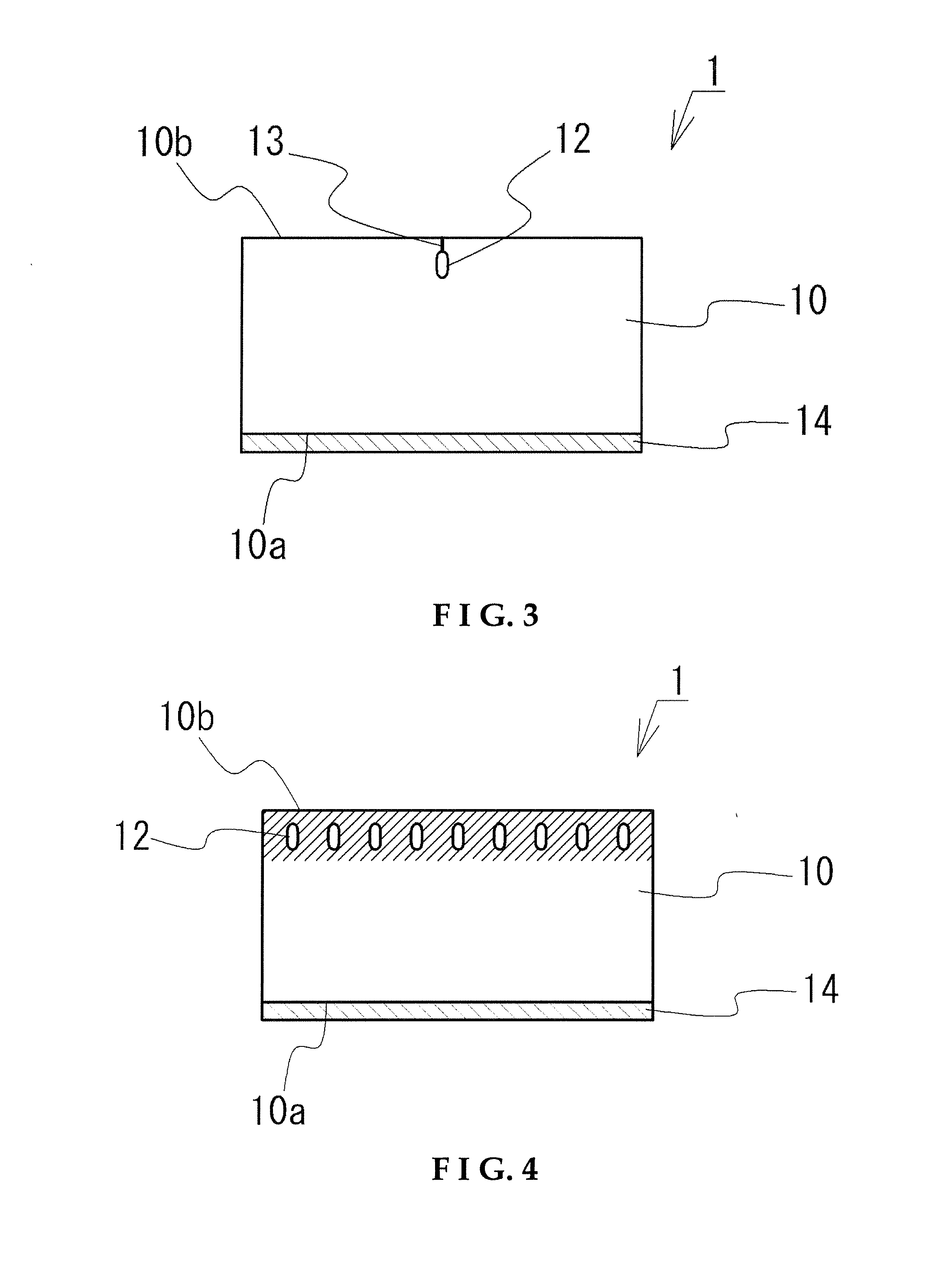
[0070]A wafer was prepared in which a GaN-based semiconductor layer was formed on one main face of a sapphire substrate with a thickness of approximately 85 μm. The semiconductor layer was produced by laminating an n-type semiconductor layer, a light emitting layer, and a p-type semiconductor layer in that order, starting from the sapphire substrate side, on the (0001) plane of the sapphire substrate.

[0071]After this, part of the light emitting layer and p-type semiconductor layer are removed to expose the n-type semiconductor layer, and an n electrode is formed on the n-type semiconductor layer surface, and a p electrode on the p-type semiconductor layer surface.

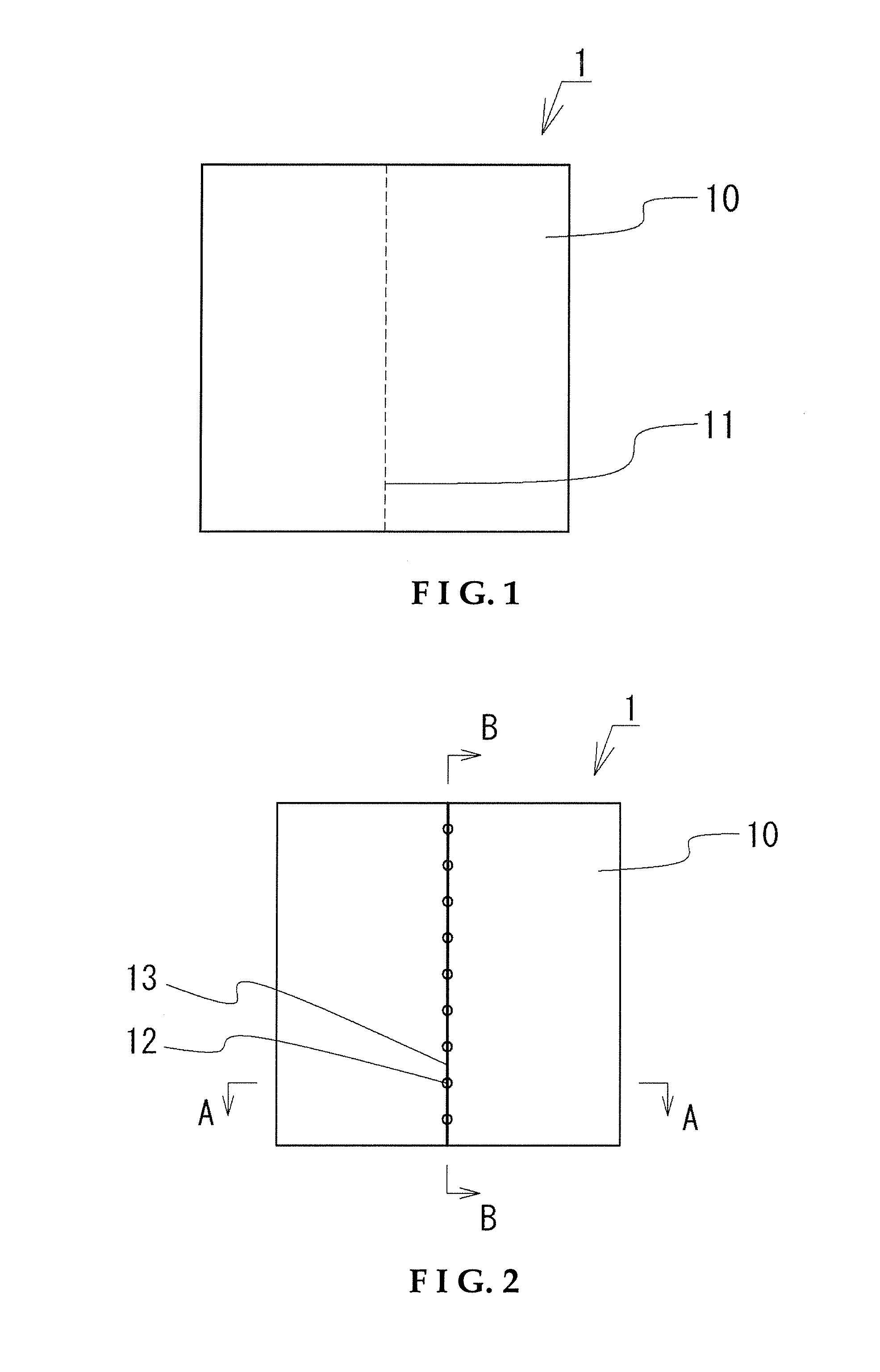
[0072]To obtain a substantially square element measuring approximately 250 μm on one side, the intended dividing lines of the wafer were set in two directions, one substantially parallel and one substantially perpendicular to the a axis of the sapphire substrate, and a pulsed laser beam was directed along each of the intend...

example 2

[0076]In this example, semiconductor elements are manufactured in the same manner as in Example 1, except that the distance between the focal positions of the laser beam is set to approximately 5 μm in irradiation with the laser beam along an intended dividing line substantially parallel to the a axis.

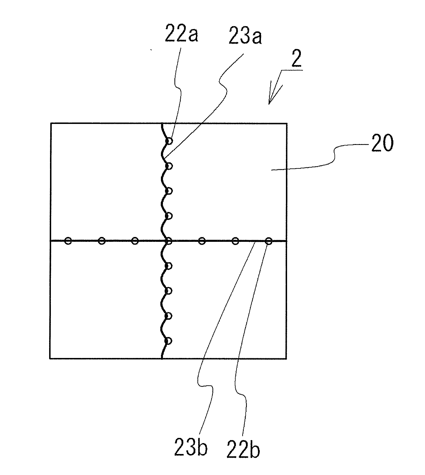
[0077]After laser irradiation, the sapphire substrate surface is observed, which confirmed the presence of substantially circular processed portions and a fissure extending from the processed portions, and confirmed that at least part of the fissure ran so as to link the processed portions on the substrate surface. After wafer division the semiconductor elements thus obtained are observed, which revealed that the element side faces is divided substantially perpendicular to the sapphire substrate surface.

[0078]The manufacturing method of the illustrated embodiments can be applied to elements that are made into elements by the division of a wafer having a substrate. It can be applied to ...


PUM

PropertyMeasurementUnit
Fractionaaaaaaaaaa
Fractionaaaaaaaaaa
Diameteraaaaaaaaaa

Abstract

A method for manufacturing a semiconductor element of the present invention, has: a laser irradiation step of focusing a pulsed laser beam inside of a substrate constituting a wafer, thereby forming a plurality of isolated processed portions along an intended dividing line inside of the substrate, and creating a fissure that runs from the processed portions at least to the surface of the substrate and links adjacent processed portions; and a wafer division step of dividing the wafer along the intended dividing line.

Description

CROSS-REFERENCE TO RELATED APPLICATIONS[0001]This national phase application claims priority to Japanese Patent Application No. 2009-041966 filed on Feb. 25, 2009. The entire disclosure of Japanese Patent Application No. 2009-041966 is hereby incorporated herein by reference.TECHNICAL FIELD[0002]The present invention relates to a method for manufacturing a semiconductor element, and more particularly relates to a semiconductor element manufacturing method comprising a step of dividing a wafer that includes a substrate.BACKGROUND ART[0003]The manufacture of a semiconductor element includes a step of dividing a wafer into element chips, and a method in which separation grooves are formed with a cutter, dicer, or the like and the pieces snapped apart has been used to divide these element chips. A method has been proposed in recent years in which a laser beam is used instead of a cutter or dicer to form separation grooves or the like, and the chips are then broken apart, but with a meth...

Claims


Application Information

Patent Timeline
IPC IPC(8): H01L21/78H01L27/12
CPCB23K26/0057B28D5/0011H01L21/78B23K26/0042B23K26/0072B23K2201/40H01L29/0657H01L33/0095B23K26/0006B23K26/53B23K26/3568B23K2101/40B23K2103/56B23K26/073B23K26/38H01L21/302H01L21/304H01L21/30625
Inventor TAMEMOTO, HIROAKI
Owner NICHIA CORP
Why Eureka
Try Eureka