Laser beam machining method for wafer

Active Publication Date: 2009-01-01
DISCO CORP
View PDF8 Cites 33 Cited by
  • Summary
  • Abstract
  • Description
  • Claims
  • Application Information

AI Technical Summary

Benefits of technology

[0041]According to the above-described embodiment, the non-cracked layers53 where the cracked layer is absent are provided between the plurality of composite layers (denatured layer 50+cracked layer 51, each) 52 formed inside the wafer 1 by the first laser beam irradiation step, and, due to the influences of crystal defects extending from the cracked layers 51 or the like, multiple photon absorption would not take place and denatured layers would not easily be formed in these non-cracked layer portions even upon irradiation thereof with the laser beam. However, the irradiation with the laser beam is expected to have the action of extending those cracked layers 51 extending from the denatured layers 50 which have already been present. In the second laser beam irradiation step, the non-cracked layer 53 is irradiated with the laser beam, whereby the cracked layer 51 of a given composite layer 52 is extended to the denatured layer 50 of the adjacent composite layer 52. This ensures that some of the cracked layers 51 formed in the first laser beam irradiation step are caused to reach the denatured layers 50 of the adjacent composite layers 52, so that splitting of the wafer 1 can be carried out easily and smoot

Problems solved by technology

This is disadvantageous from the viewpoint of increasing the number of chips obtained from a single wafer as much as possible to thereby enhance productivity.
However, in the case of splitting the wafer by the laser beam machining method while the wafer is kept comparatively thick without being thinned, there would be a problem that formation of one denatured layer through one-time irradiation with the laser beam for each of the planned dividing lines may make smooth dividing of the wafer impossible, due to the small proportion of the denatured layer based on the wafer thickness.
This means the need to repeat the laser beam irradiation 18 times for each of the planned dividing lines, so that the number of times of irradiation is too large to obtain good machining efficiency.
However, even by irradiation with the laser beam with a wavelength of 1342 nm, it is in practice difficult to form a multiplicity of denatured layers proximate to each other in the thickness direction of the wafer.
Therefore, if the multiplicity of denatured layers cannot be form

Method used


Image

  • Laser beam machining method for wafer
  • Laser beam machining method for wafer
  • Laser beam machining method for wafer

Examples


example 1

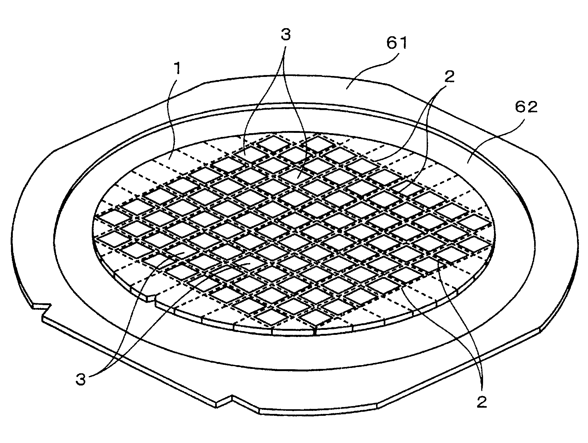
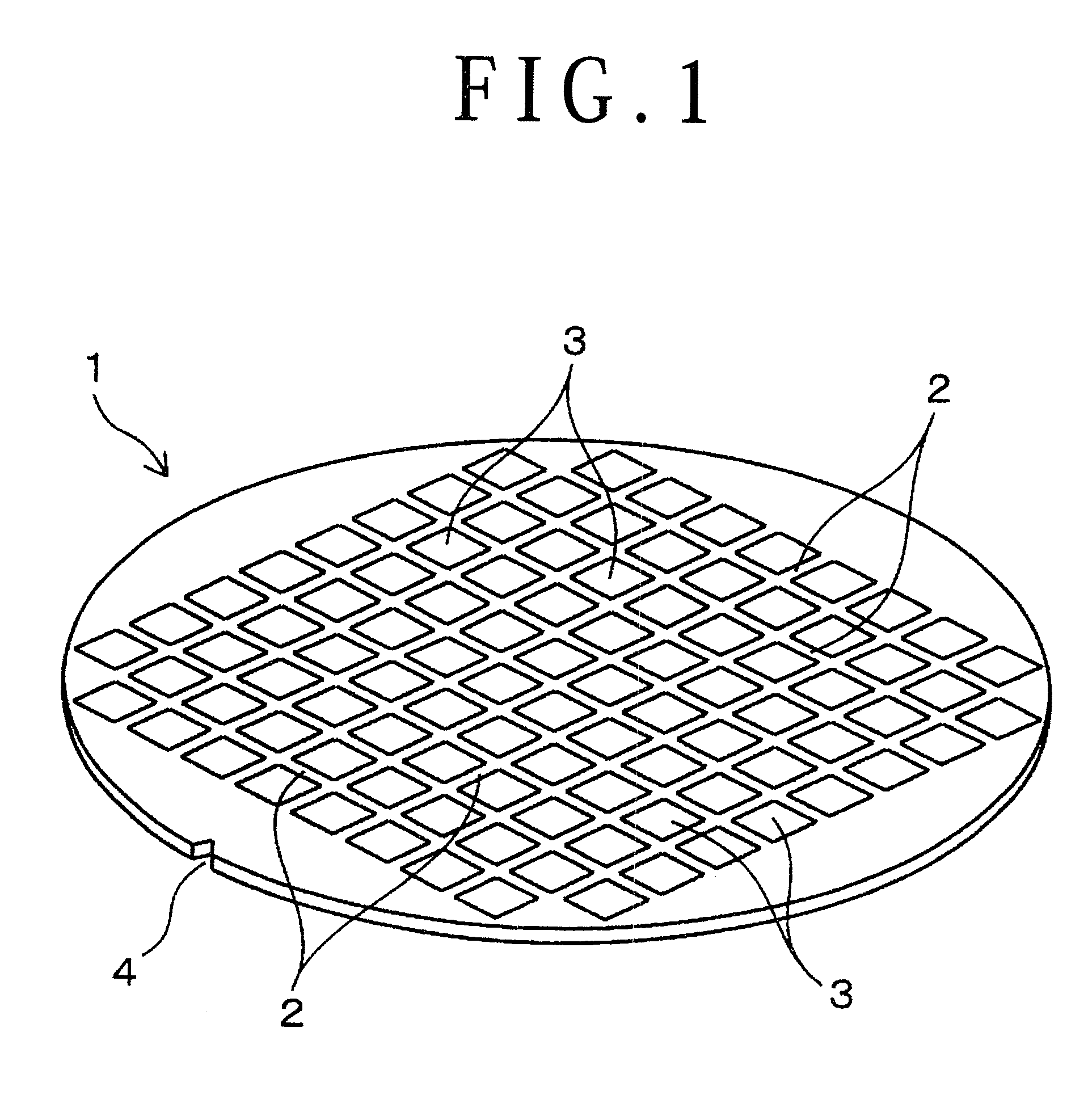
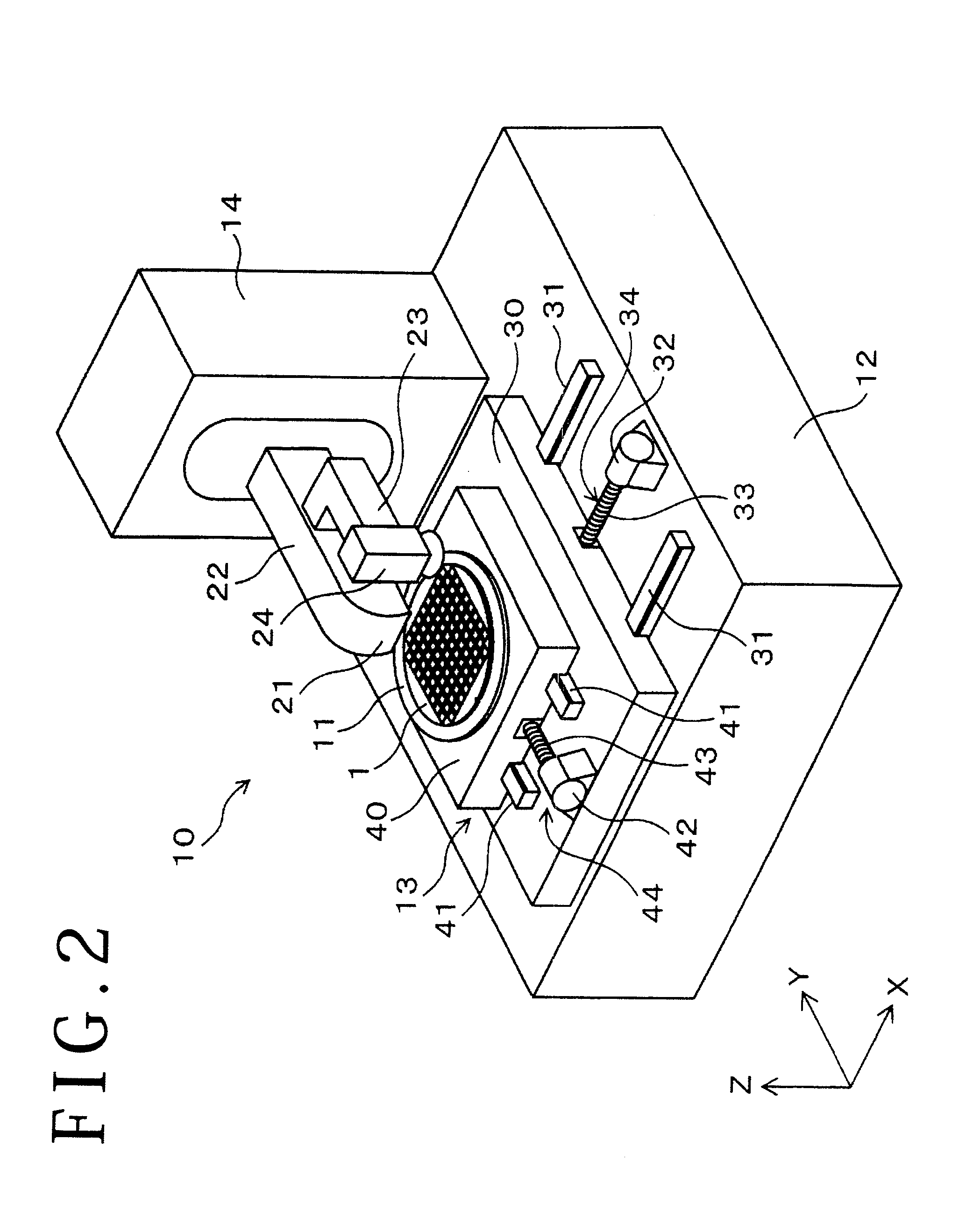
[0044]A silicon wafer at a blank material stage having a diameter of 150 mm and a thickness of 400 μm was prepared as a sample. The wafer is a so-called “mirror wafer,” i.e., a wafer not provided on its face-side surface with a device pattern which might be obtained by providing electronic circuits in chip regions demarcated by grid-like planned dividing lines. The wafer was set on a chuck table of a laser beam machining apparatus the same as that shown in FIG. 2, with its face side up. The wafer was provided with virtual planned dividing lines at intervals of 1.5 mm, and, along all the virtual planned dividing lines, five composite layers (denatured layer+cracked layer, each) were formed stepwise at intervals of 20 μm, starting from a wafer inside position proximate to the back-side surface of the wafer. Next, three of the four non-cracked layers between the composite layers were subjected to irradiation with the laser beam, to form extended cracked layers. In other words, the lase...

example 2

[0053]A mirror wafer substantially the same as that in Example 1 was actually provided in its face-side surface with grid-like planned dividing lines at intervals of 1.5 mm, and suitable electronic circuits were formed in chip regions demarcated by the planned dividing lines, whereby a “pattern wafer” provided with device patterns were prepared as a sample. The wafer was irradiated with a laser beam in quite the same manner as in Example 1, whereby five composite layers (denatured layer+cracked layer, each) plus three extended cracked layers were formed inside the wafer along each of the planned dividing lines.


PUM

PropertyMeasurementUnit
Wavelengthaaaaaaaaaa
Forceaaaaaaaaaa

Abstract

A laser beam machining method for a wafer, wherein an operation of irradiating the inside of a wafer with a laser beam L along each of planned dividing lines is repeated a plural number of times from a position proximate to a back-side surface of the wafer toward a face-side surface of the wafer so that a plurality of composite layers each including a denatured layer and a cracked layer extending from the denatured layer toward the face-side surface are formed stepwise at intervals (first laser beam irradiation step). Subsequently, each of some of non-cracked layers between the composite layers is irradiated with the laser beam L so as to extend the cracked layer of a given one of the composite layers and to cause the cracked layer to reach the denatured layer of the composite layer which is adjacent to the given one composite layer. The denatured layers and the cracked layers which are sufficient for enabling the wafer to be split are formed by a reduced number of laser beam irradiation operations.

Description

BACKGROUND OF THE INVENTION[0001]1. Field of the Invention[0002]The present invention relates to a laser beam machining method in which a wafer such as a semiconductor wafer is irradiated with a laser beam along each of planned dividing lines formed in the wafer, whereby denatured layers are formed inside the wafer along each of the planned dividing lines.[0003]2. Description of the Related Art[0004]In the semiconductor device chip manufacturing process, planned dividing lines arranged in a grid-like form are formed in a face-side surface of a substantially circular disk-like semiconductor wafer to demarcate a plurality of rectangular regions in the face-side surface, then electronic circuits such as ICs (Integral Circuit) and LSIs (Large Scale Integration) and / or minute electromechanical devices called MEMS (Micro Electro Mechanical System) are formed in the rectangular regions, and thereafter the wafer is cut along the planned dividing lines to obtain semiconductor chips based on ...

Claims


Application Information

Patent Timeline
IPC IPC(8): H01L21/268B23K26/364B23K26/38B28D5/00
CPCB23K26/0057H01L21/78B28D5/0011B23K26/4075B23K26/40B23K26/53B23K2103/50
Inventor KOBAYASHI, SATOSHI
Owner DISCO CORP
Why Eureka
Try Eureka