

Light emitting device and sealing material
- Summary
- Abstract
- Description
- Claims
- Application Information
AI Technical Summary
Benefits of technology
Problems solved by technology
Method used
Image

Examples
first embodiment
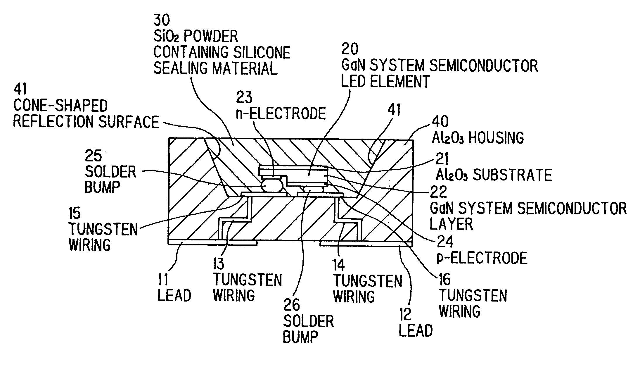
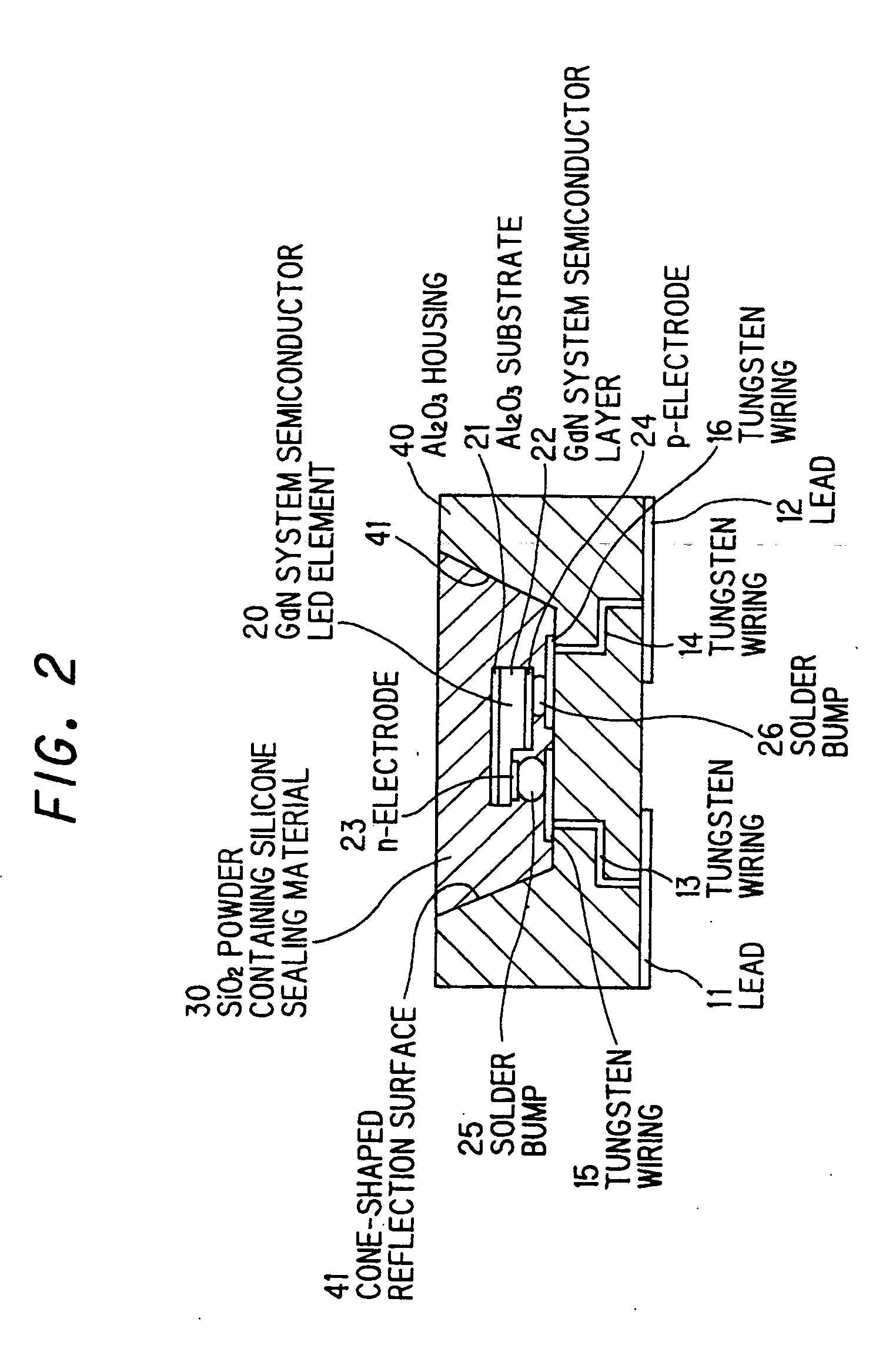
[0069]FIG. 2 is a cross sectional view showing a light emitting device in the first preferred embodiment according to the invention.
[0070] The light emitting device is composed of a ceramic (Al2O3) housing 40, a GaN system semiconductor light emitting element 20, and a silica glass powder containing silicone sealing material 30 that SiO2 (silica glass with a refractive index of n=1.46) powder is as a filler mixed into silicone (with a refractive index of n=1.46).
[0071] The Al2O3 housing 40 is provided with a cone-shaped reflection surface 41 metallized, and tungsten wirings 15, 16 as a conducting portion formed by printing at the bottom so as to form a mounting part. The tungsten wirings 15, 16 are electrically connected with leads 11, 12 at the back face of the Al2O3 housing 40 through tungsten wirings 13, 14 at the wall of via holes. The Al2O3 housing 40 may be formed concave other than having the cone-like slope as shown in FIG. 2.
[0072] The GaN system semiconductor light emit...
second embodiment
[0079]FIG. 3 is a cross sectional view showing a light emitting device in the second preferred embodiment according to the invention. In FIG. 3, like components are indicated by the same numerals as used in FIG. 2 and the explanations thereof are omitted below.
[0080] The light emitting device of the second embodiment is composed of the ceramic (Al2O3) housing 40, the GaN system semiconductor light emitting element 20, and SiO2 (silica glass) powder containing silicone sealing materials 31, 32.
[0081] The ceramic (Al2O3) housing 40 and the GaN system semiconductor light emitting element 20 are the same as described in the first embodiment in FIG. 2.
[0082] The silica glass powder containing silicone sealing material 31 of lower layer is made of the silica glass powder containing silicone as described in the first embodiment in FIG. 2. The silica glass powder containing silicone sealing material 32, which is formed on the lower silica glass powder containing silicone sealing material...
third embodiment
[0089]FIG. 4 is a cross sectional view showing a light emitting device in the third preferred embodiment according to the invention. In FIG. 4, like components are indicated by the same numerals as used in FIG. 2 and the explanations thereof are omitted below.
[0090] The light emitting device of the third embodiment is common to that of the second embodiment in FIG. 3 in that it has the GaN system semiconductor light emitting element 20, the lower SiO2 (silica glass) powder containing silicone sealing material 31 and the upper SiO2 (silica glass) powder containing silicone sealing material 32 (with the phosphor contained therein) However, the former is different from the latter in that it has a copper housing 70 and a glass epoxy resin material 60 in place of the Al2O3 housing 40.
[0091] In this light emitting device, the copper housing 70 is a cone-shaped reflection surface 71, and it has the glass epoxy resin material 60 formed around there. An AlN submount 100 is provided at the ...
PUM
 Abstract
Description
Claims
Application Information