
Configurable embedded processor

a technology of embedded processors and memory systems, applied in the direction of memory address formation, micro-instruction address formation, instruments, etc., can solve the problems of dual port memory operating frequency, dual port memory operation at lower frequencies, and additional complexity of dual port memory, so as to increase the utilization of cpu and dma controller

Inactive Publication Date: 2005-08-11
INFINEON TECH AG
View PDF9 Cites 18 Cited by
  • Summary
  • Abstract
  • Description
  • Claims
  • Application Information

AI Technical Summary

Benefits of technology

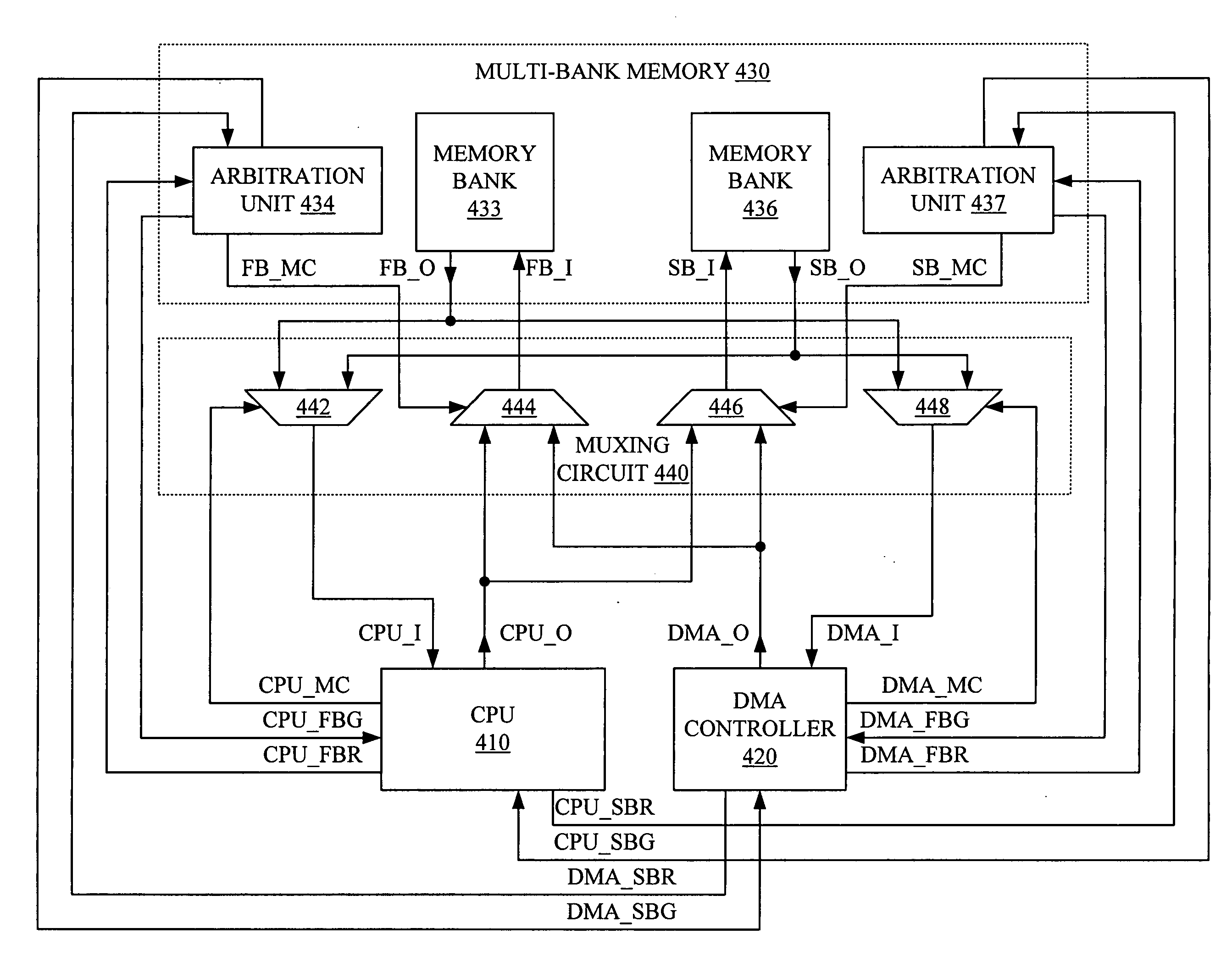
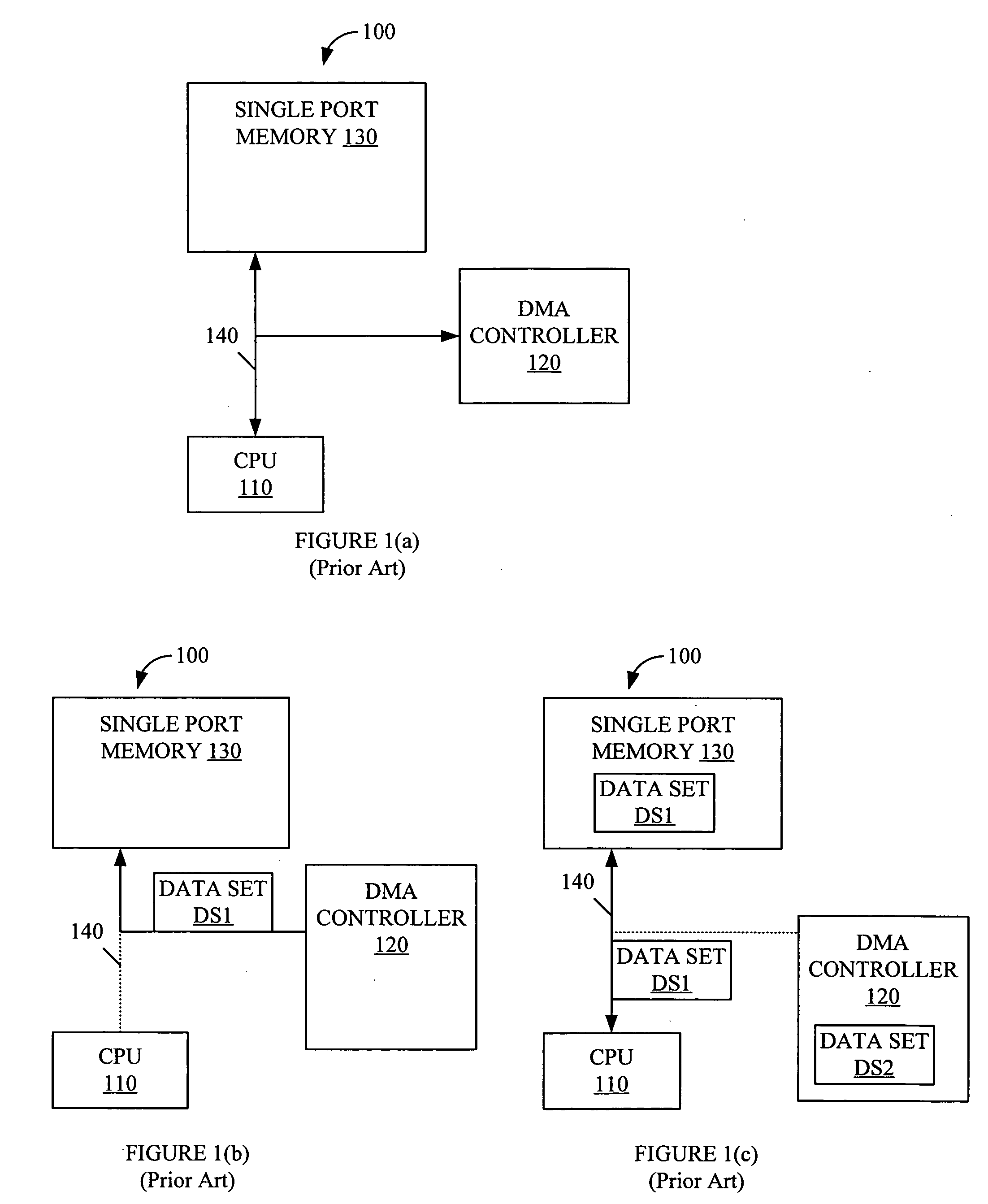
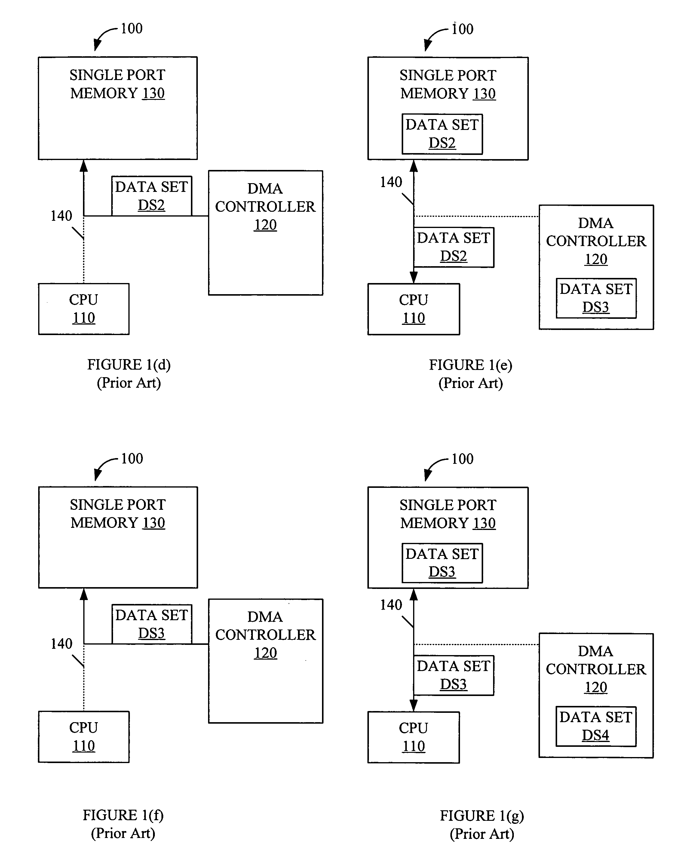
[0008] Accordingly, a microprocessor system in accordance with the present invention, uses multiple single port memory banks to allow efficient use of the CPU and the DMA controller as well as other bus masters. For example, in one embodiment of the present invention, as the CPU is processing a first data set in the first memory bank, the DMA controller can be writing a second data set into the second memory bank. Once the CPU is finished processing the first data set and the DMA controller has finished writing the second data set, the CPU can process the second data set in the second memory bank while the DMA controller writes a third data set into the first memory bank. By using the memory banks in parallel, the present invention provides higher utilization of the CPU and the DMA controller.

Problems solved by technology

Furthermore, dual port memories have much higher power consumption and operate at lower frequencies than single port memories.
In addition dual port memories have additional complexities such as port contention for the same memory addresses that must be resolved.

Method used


Image

  • Configurable embedded processor
  • Configurable embedded processor
  • Configurable embedded processor

Examples


Embodiment Construction

[0016] As explained above, conventional microprocessor systems have low utilization of the CPU due to memory bottlenecks caused by sharing a single port memory with a DMA controller. While using a dual port memory provides higher utilization, the cost in silicon area and power for the dual port memory prevents wide spread use of dual port memories. The present invention provides a novel microprocessor system that provides the benefits of a dual port memory system without the detriments.

[0017]FIG. 3 is a simplified block diagram of a microprocessor system 300 in accordance with one embodiment of the present invention. Microprocessor system 300 includes a CPU 310, a DMA controller 320, a multi-bank memory 330 having a first memory bank 333 and a second memory bank 336, and a muxing circuit 340. Muxing circuit 340 couples CPU 310 and DMA controller 320 to memory banks 333 and 336. Muxing circuit 340 could be for example, a multiplexer or a crossbar switch. For clarity, the sample embo...


PUM


Abstract

A microprocessor system includes a multi-bank memory having a first memory bank and a second memory bank, a muxing circuit, a CPU and a DMA controller. The muxing circuit allows the CPU to access one of the memory bank while allowing the DMA controller access to the other memory bank at the same time. Thus, the microprocessor system needs to process multiple data sets, the CPU can be processing a first data set in the first memory bank while the DMA controller is writing a second data set in the second memory bank. When the CPU is finished processing the first data set and the DMA controller is finished writing the second data set, the muxing circuit is reconfigured so that the CPU can process the second data set in the second memory bank and the DMA controller can write a third data set in the first memory bank.

Description

FIELD OF THE INVENTION [0001] The present invention relates to microprocessor systems, and more particularly to a memory system for a microprocessor system to reduce memory contention between a CPU and a DMA controller. BACKGROUND OF THE INVENTION [0002]FIG. 1(a) illustrates a conventional microprocessor system 100 having a central processing unit (CPU) 110, a direct memory access (DMA) controller 120, a single port memory 130 and a memory bus 140. CPU 110 and DMA controller 120 are coupled to single port memory 130 by memory bus 140. In general both CPU 110 and DMA controller 120 are memory access devices that are considered bus master, while single port memory 130 is considered a slave device that is being shared by the bus masters. [0003] In many situations, particularly for digital signal processing, DMA controller 120 must store a data set in single port memory 130 for CPU 110 to process. Ideally, DMA controller 120 would store a second data set for CPU 110 after writing the fi...

Claims


Application Information

Patent Timeline
Patent Type & Authority Applications(United States)
IPC IPC(8): G06F12/00G06F13/16G06F15/78
CPCG06F15/7857G06F13/1647
Inventor OBER, ROBERT E.OBERLAENDER, KLAUS J.
Owner INFINEON TECH AG
Learn More