Methods of fabricating vertical carbon nanotube field effect transistors for arrangement in arrays and field effect transistors and arrays formed thereby

a technology of field effect transistor and vertical carbon nanotube, which is applied in the field of vertical carbon nanotube field effect transistor and arrays formed by it, can solve the problems of reducing the number of carbon nanotubes, limiting the size limitations of traditional materials and the cost of lithographic patterning, and unable to meet the requirements of mass production

Inactive Publication Date: 2005-08-18
GLOBALFOUNDRIES US INC
View PDF16 Cites 32 Cited by
  • Summary
  • Abstract
  • Description
  • Claims
  • Application Information

AI Technical Summary

Problems solved by technology

However, continued dimensional reductions may be hampered by the size limitations associated with traditional materials and the costs associated with lithographic patterning.
Conventional manipulation or coincidental placement of car

Method used


Image

  • Methods of fabricating vertical carbon nanotube field effect transistors for arrangement in arrays and field effect transistors and arrays formed thereby
  • Methods of fabricating vertical carbon nanotube field effect transistors for arrangement in arrays and field effect transistors and arrays formed thereby
  • Methods of fabricating vertical carbon nanotube field effect transistors for arrangement in arrays and field effect transistors and arrays formed thereby

Examples


Embodiment Construction

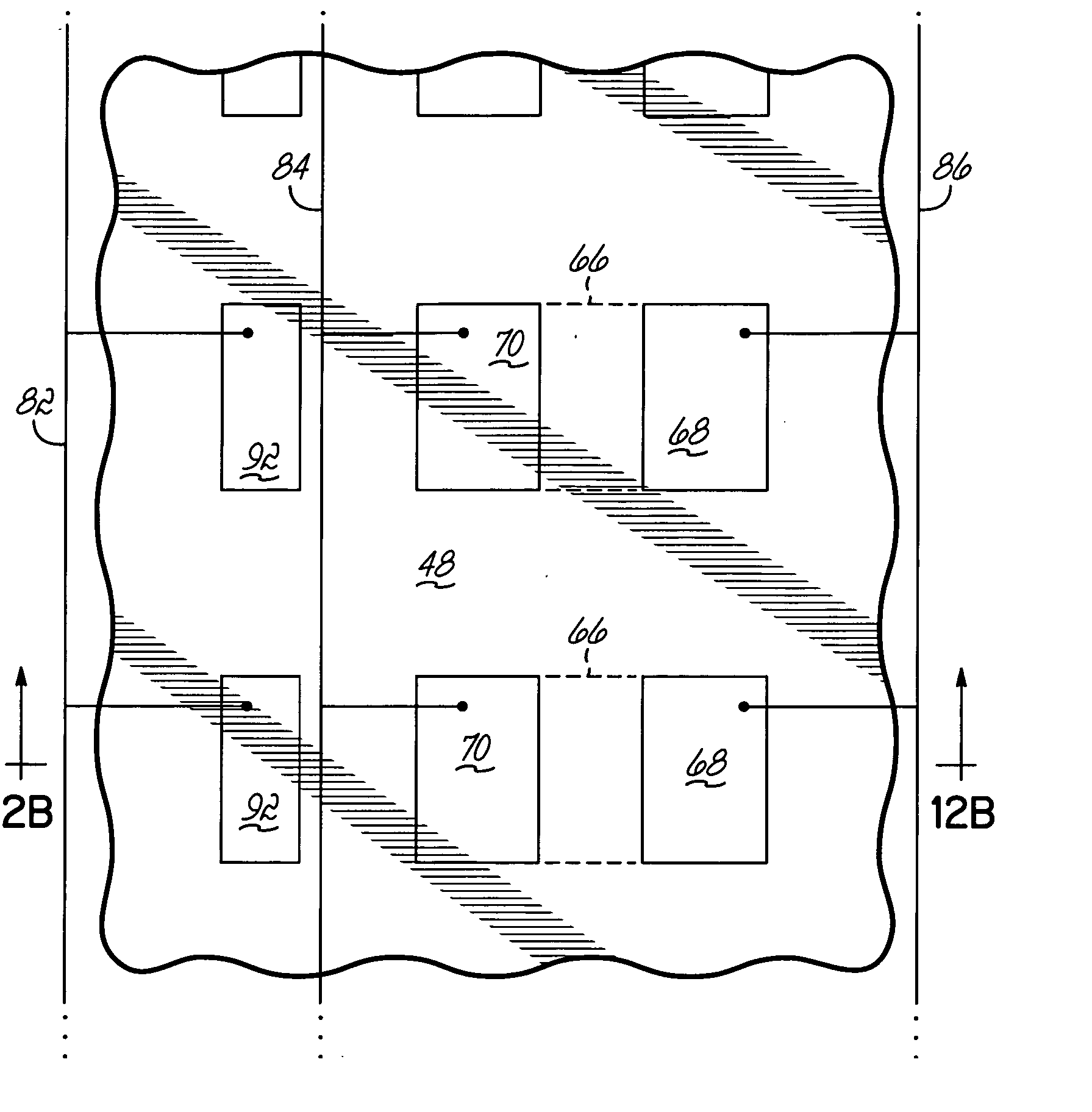
[0035] The invention in its various embodiments provides methods for forming arrays of field effect transistors (FET's) incorporating semiconducting carbon nanotubes as a channel region and, optionally, conducting carbon nanotubes as a component of a gate contact and / or a source contact. Adjacent FET's are spaced apart such that, as the carbon nanotubes lengthen, the flow of CVD reactant(s) to a catalyst material supporting nanotube synthesis does not become restricted. Because the nanotube synthesis is unencumbered by significant flow restrictions, the carbon nanotubes may be grown at a higher rate to a greater length, and arrays of FET's may be formed by appropriate mass production techniques.

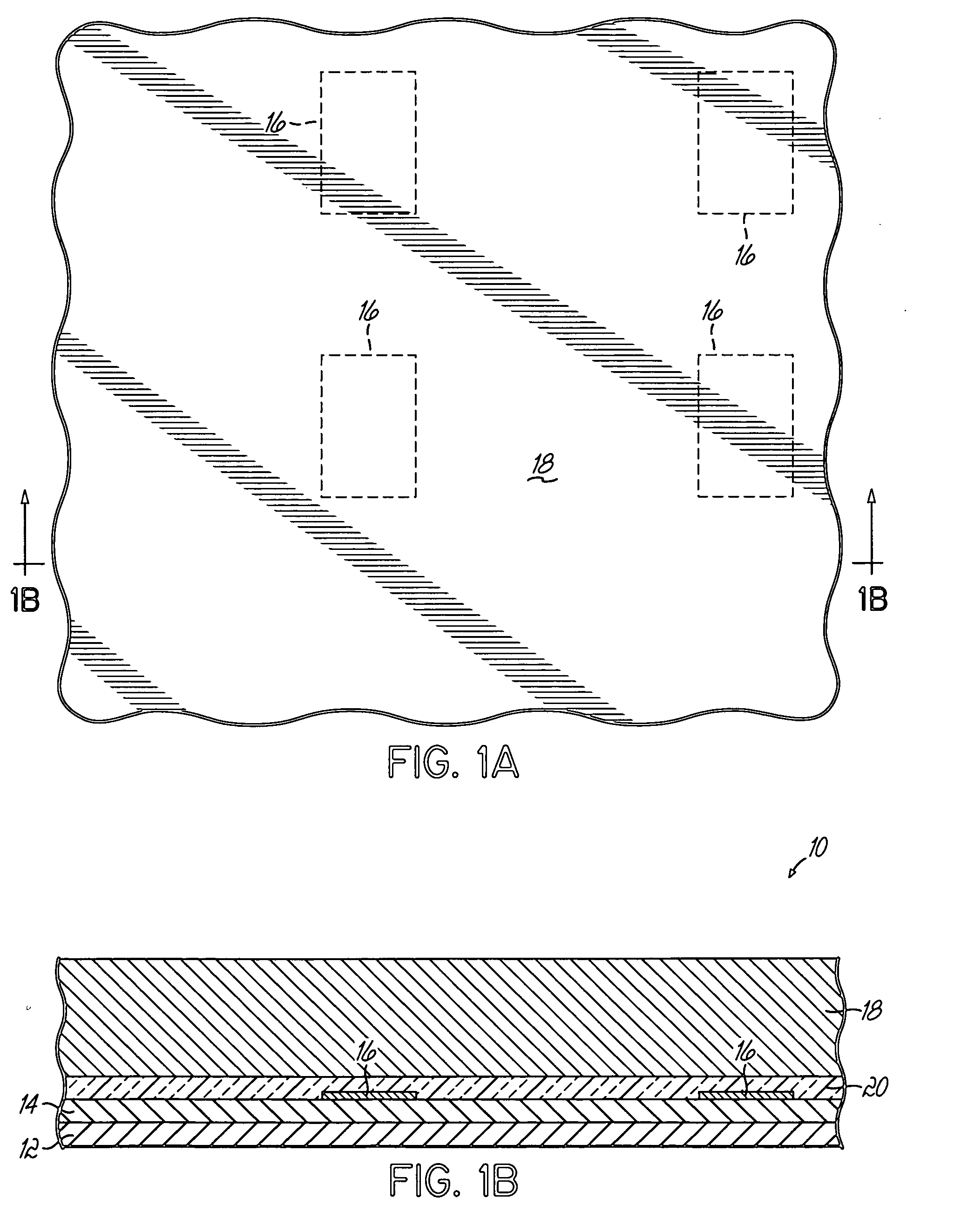
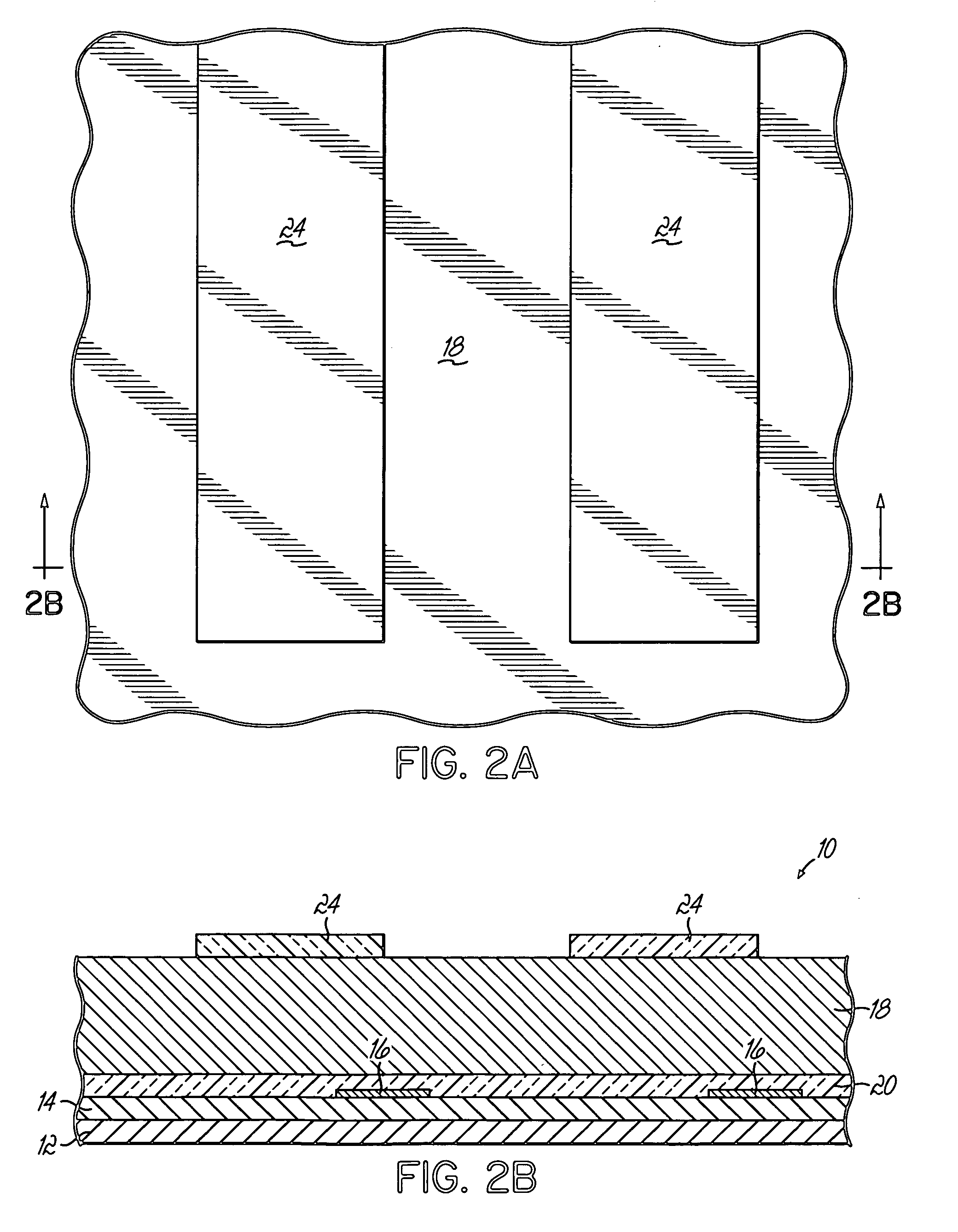
[0036] With reference to FIGS. 1A and 1B, a layer stack 10 is formed on a substrate 12 covered by multiple parallel rows or stripes of a conductive layer 14 composed of a conducting material that participates in a source / drain connection in the completed device structure 54 (FIGS. 9A and 9B)...


PUM


Abstract

A method for forming carbon nanotube field effect transistors, arrays of carbon nanotube field effect transistors, and device structures and arrays of device structures formed by the methods. The methods include forming a stacked structure including a gate electrode layer and catalyst pads each coupled electrically with a source/drain contact. The gate electrode layer is divided into multiple gate electrodes and at least one semiconducting carbon nanotube is synthesized by a chemical vapor deposition process on each of the catalyst pads. The completed device structure includes a gate electrode with a sidewall covered by a gate dielectric and at least one semiconducting carbon nanotube adjacent to the sidewall of the gate electrode. Source/drain contacts are electrically coupled with opposite ends of the semiconducting carbon nanotube to complete the device structure. Multiple device structures may be configured either as a memory circuit or as a logic circuit.

Description

FIELD OF THE INVENTION [0001] The invention relates to semiconductor device fabrication and, more particularly, to methods of constructing vertical carbon nanotube field effect transistors and arrays thereof, and device structures and arrays of device structures formed by such methods. BACKGROUND OF THE INVENTION [0002] Traditional field effect transistors (FET's) are familiar conventional devices commonly incorporated as a fundamental building block into the intricate circuitry of integrated circuit (IC) chips. Downward scaling of FET dimensions has improved circuit performance and increased the functional capability of FET's packed on an IC chip. However, continued dimensional reductions may be hampered by the size limitations associated with traditional materials and the costs associated with lithographic patterning. [0003] Carbon nanotubes are nanoscale high-aspect-ratio cylinders consisting of hexagonal rings of carbon atoms that may assume either a semiconducting electronic st...

Claims


Application Information

Patent Timeline
IPC IPC(8): G11C13/02H01L21/336H01L27/28H01L51/05H01L51/30H01L51/40
CPCB82Y10/00G11C13/025H01L29/0665H01L29/0673H01L29/0676Y10S977/734H01L29/66409H01L29/772H01L51/0048H01L51/057H01L29/125H10K85/221H10K10/491H01L21/18H01L29/775B82Y40/00
Inventor FURUKAWA, TOSHIHARUHAKEY, MARK CHARLESHOLMES, STEVEN JOHNHORAK, DAVID VACLAVKOBURGER, CHARLES WILLIAM IIIMITCHELL, PETER H.NESBIT, LARRY ALAN
Owner GLOBALFOUNDRIES US INC
Why Eureka
Try Eureka