Semiconductor device having multilayer structure and method for manufacturing thereof

Active Publication Date: 2005-08-18
RENESAS ELECTRONICS CORP
View PDF3 Cites 33 Cited by
  • Summary
  • Abstract
  • Description
  • Claims
  • Application Information

AI Technical Summary

Benefits of technology

[0015] A more specific object of the present invention is to provide a semiconductor device

Problems solved by technology

However, with the recent tendency to make wiring patterns finer, various problems have arisen in lithography techniques.
In some cases, the method for wiring design on a square grid (also called “uniform grid”) in particular cannot be used.
That is, a problem arises that a wiring design cannot be made on a square grid because the CD shift becomes larger than the wiring space margin.
As described above, it has been found that there is a problem with an application of the mask bias technique to wiring layout on a square grid when the width of isolated wirings is smaller than 0.15 μm.
It is difficult to correct the CD shift with the mask bias technique or the method of adding a correction pattern when a finer pattern is used.
That is, while the CD shift increases as the wiring width is reduced, the wiring space margin is reduced whe

Method used


Image

  • Semiconductor device having multilayer structure and method for manufacturing thereof
  • Semiconductor device having multilayer structure and method for manufacturing thereof
  • Semiconductor device having multilayer structure and method for manufacturing thereof

Examples


first embodiment

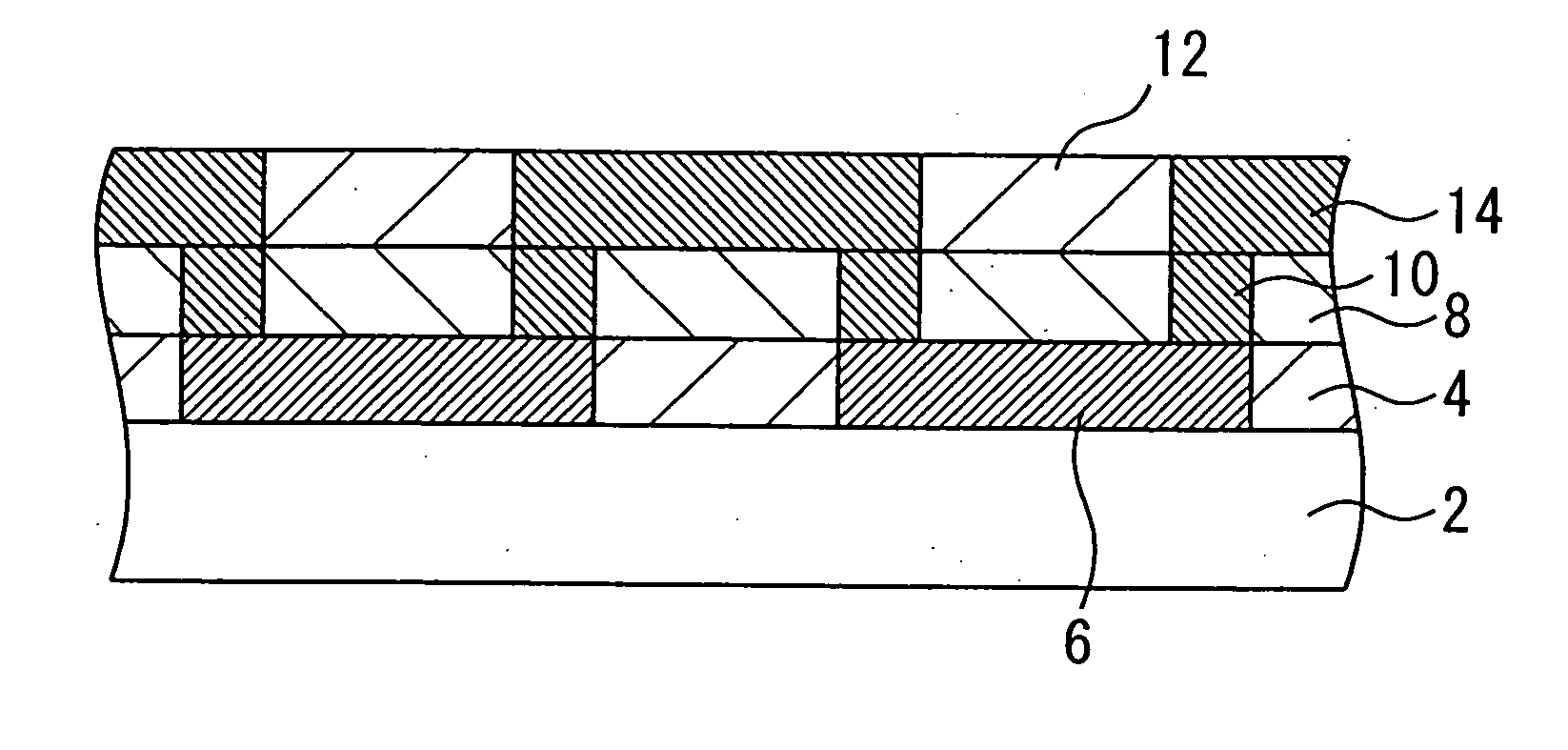
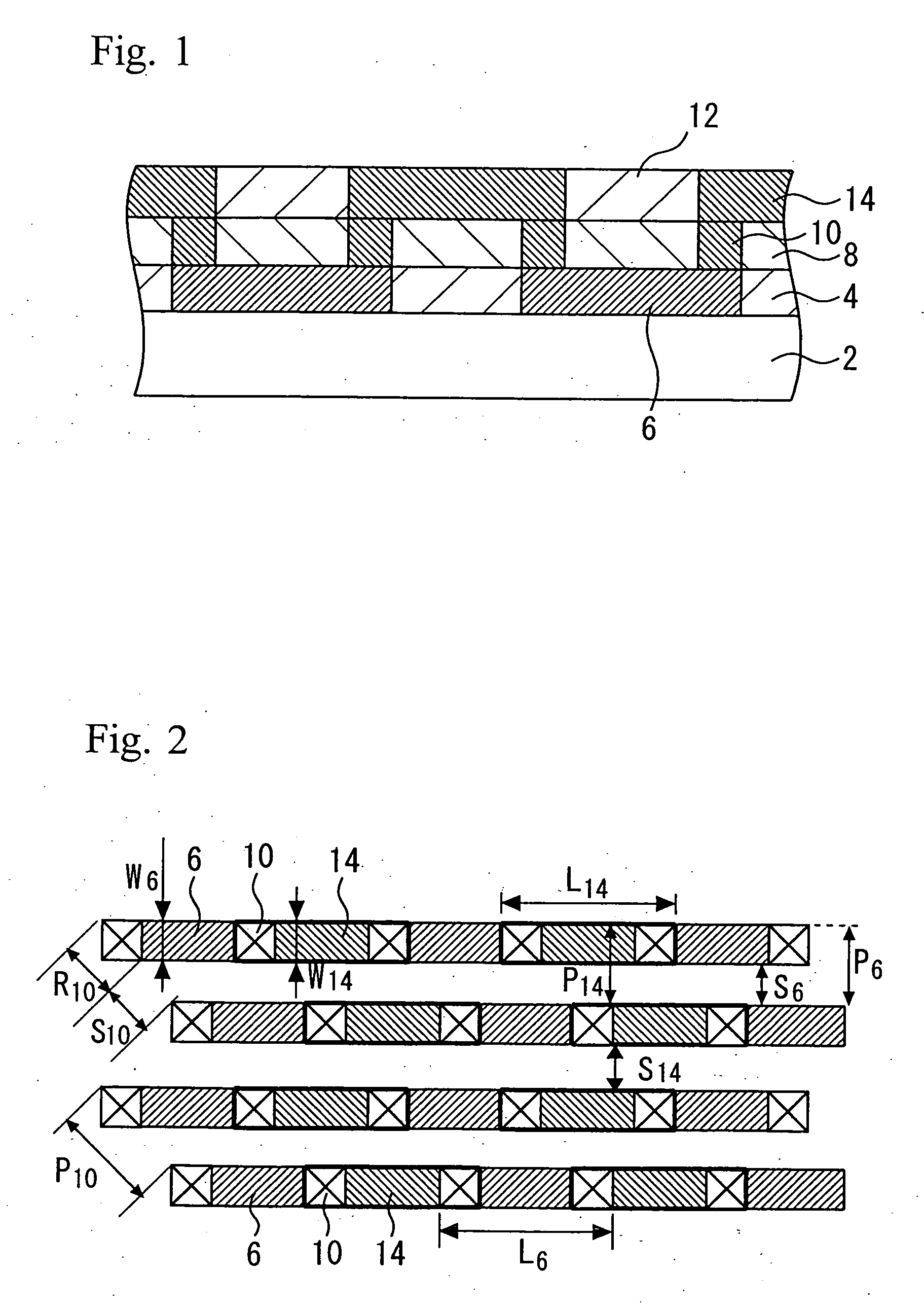
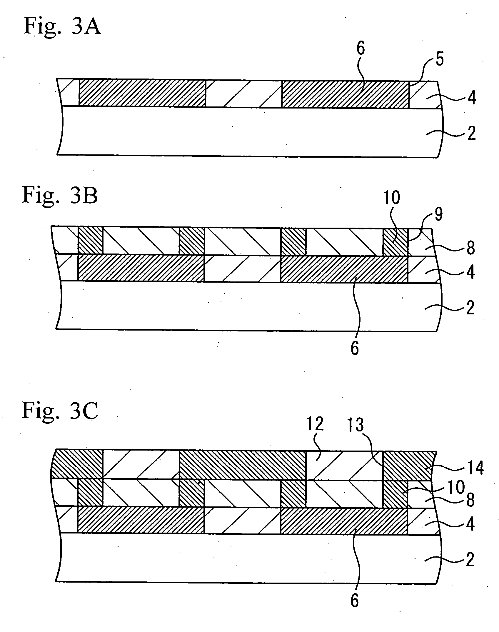
[0038]FIG. 1 is a schematic cross-sectional view of a semiconductor device according to a first embodiment of the present invention, and FIG. 2 is a schematic top view of the wiring structure of the semiconductor device in the first embodiment of the present invention.

[0039] As shown in FIGS. 1 and 2, transistors, wiring layers, etc., (not shown) are formed as required on a substrate 2 of the semiconductor device in the first embodiment. A first interlayer dielectric film 4 constituting a first wiring layer is also formed on the substrate 2. First wirings 6 are formed in the first interlayer dielectric film 4. The thickness of the first interlayer dielectric film 4 and the first wirings 6 is about 200 nm. A second interlayer dielectric film 8 constituting a via layer is formed on the first interlayer dielectric film 4 and the first wirings 6. Vias 10 are formed in the second interlayer dielectric film 8 so as to be connected to the first wirings 6 through the second interlayer diel...

second embodiment

[0067]FIG. 9 is a schematic cross-sectional view of a semiconductor device according to a second embodiment of the present invention. FIG. 10 is a schematic top view of the wiring structure of the semiconductor device in the second embodiment.

[0068] As shown in FIGS. 9 and 10, the semiconductor device in the second embodiment is similar to the semiconductor device in the first embodiment described above. However, vias of the semiconductor device in the second embodiment are formed so as to be larger than the wiring width. Concrete description of this will be made below.

[0069] In the semiconductor device in the second embodiment, a first interlayer dielectric film 24 constituting a first wiring layer is formed on the substrate 22, as is that of the semiconductor device in the first embodiment. First wirings 26 are formed in the first interlayer dielectric film 24. The thickness of the first interlayer dielectric film 24 and the first wirings 26 is about 200 nm. A second interlayer ...


PUM


Abstract

A semiconductor device having a first wiring layer including first wirings on a substrate, a contact layer on the first wiring layer and including contacts connected to the first wirings, and a second wiring layer on the contact layer and including second wirings connected to the contacts. Contact pitch is larger than the minimum wiring pitch of the first wirings or the minimum wiring pitch of the second wirings.

Description

FIELD OF THE INVENTION [0001] The present invention relates to a semiconductor device and to a method for manufacturing there of. More particularly, the present invention relates to a semiconductor device having a multilayer structure including stacked wiring layers and contacts which connect the wiring layers, and to a method for manufacturing thereof. DESCRIPTION OF THE BACKGROUND ART [0002] In recent years, with the development of semiconductor devices improved in multifunctionality and packaging density, a multilayer wiring structure in which a plurality of wiring layers are vertically stacked has found great use. In most cases of forming contacts used for connection of stacked wiring layers or the like, holes for wiring or contacts are formed in an interlayer dielectric film based on a design rule for the multilayer wiring structure, and conductive members or the like are embedded in the holes to form the contacts. In other cases, a film of a material used for wiring and for so...

Claims


Application Information

Patent Timeline
IPC IPC(8): H01L21/3205H01L21/4763H01L21/82H01L23/48H01L23/52H01L23/522H01L23/528H01L27/118H03K19/00
CPCH01L23/5226H01L23/528H01L27/118H01L2924/0002H01L2924/00
Inventor MATSUBARA, YOSHIHISA
Owner RENESAS ELECTRONICS CORP
Why Eureka
Try Eureka