On die termination mode transfer circuit in semiconductor memory device and its method
a transfer circuit and semiconductor memory technology, applied in logic circuit coupling/interface arrangement, digital storage, instruments, etc., can solve problems such as abnormal generation of r
- Summary
- Abstract
- Description
- Claims
- Application Information
AI Technical Summary
Benefits of technology
Problems solved by technology
Method used
Image
Examples
Embodiment Construction
[0041] Hereinafter, an on die termination (ODT) mode transfer circuit for use in a semiconductor memory device in accordance with a preferred embodiment of the present invention will be described in detail referring to the accompanying drawings.
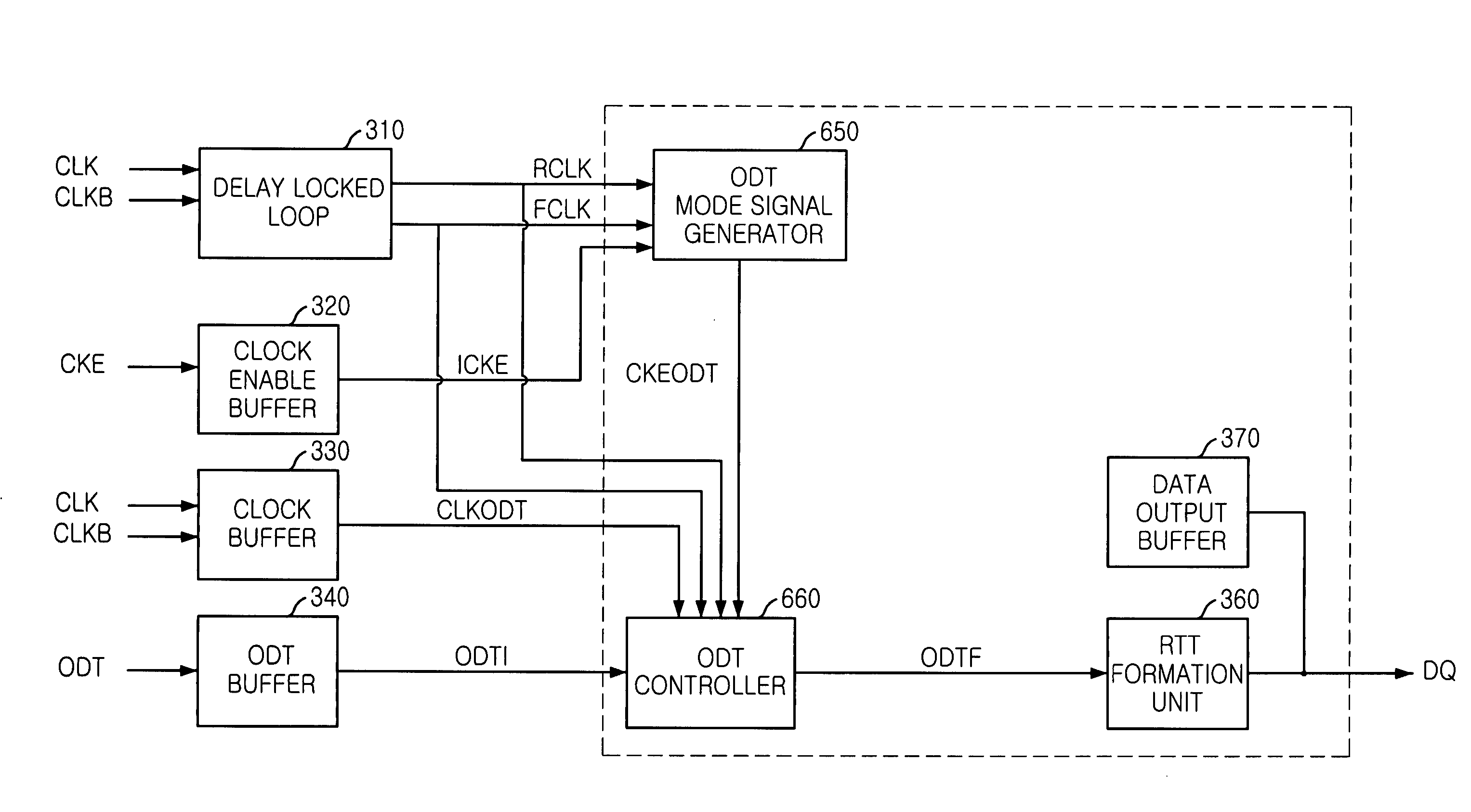
[0042]FIG. 6 is a block diagram showing an ODT mode transfer circuit in accordance with a preferred embodiment of the present invention.
[0043] As shown, the ODT mode transfer circuit includes a delay locked loop (DLL) 310, a clock enable buffer 320, a clock buffer 330, an ODT controller 350, an ODT mode signal generator 650, an ODT controller 660, an RTT formation unit 360 and a data output buffer.
[0044] The DLL 310 receives an external clock signal CLK and an external clock bar signal CLKB in order to generate a rising clock signal RCLK and a falling clock signal FCLK.
[0045] The clock enable buffer 320 buffers a clock enable signal CKE for outputting the buffered signal as a buffed clock enable signal ICKE.
[0046] The clock buffer 330 re...
PUM
 Abstract
Description
Claims
Application Information


