Fin field effect transistors having multi-layer fin patterns and methods of forming the same

a technology of fin field effect transistor and fin field effect, which is applied in the direction of transistors, semiconductor devices, electrical equipment, etc., can solve the problems of reduced transistor size, operational and structural problems, and more easily induced punch-through effects between the drain and source regions

Active Publication Date: 2005-08-25
SAMSUNG ELECTRONICS CO LTD
View PDF7 Cites 180 Cited by
  • Summary
  • Abstract
  • Description
  • Claims
  • Application Information

AI Technical Summary

Benefits of technology

[0009] In other embodiments, several first and second semiconductor patterns may be alternately stacked to increase the height of the fin pattern, and one of the first and second semiconductor patterns may reduce stress from the other of the first and second semiconductor patterns. Also, the lattice widths of the first and second patterns can be greater than the lattice width of the substrate in a direction along the channel length of the fin field effect transistor. In addition, one of the first and second semiconductor patterns may be formed of strained silicon, and the other of the first and second semiconductor patterns may be formed of silicon-germanium. The silicon-germanium pattern may reduce stress from the strained silicon pattern.
[0014] According to some embodiments, forming the fin pattern may includes forming several first and second semiconductor patterns which are alternately stacked, to increase the height of the fin pattern. One of the first and second semiconductor patterns may reduce stress from the other of the first and second semiconductor patterns. Also, the lattice widths of the first and second patterns may be greater than the lattice width of the substrate in a direction along the channel length of the fin field effect transistor. In addition, one of the first and second semiconductor patterns can be formed of strained silicon, and the other of the first and second semiconductor patterns can be formed of silicon-germanium. The silicon-germanium pattern can reduce stress from the strained silicon pattern.

Problems solved by technology

As semiconductor devices become more highly integrated, transistor size may be reduced, which may cause a variety of operational and structural problems.
For example, shorter channel length may result in more easily induced punch-through effects between the drain and source regions.
Also, controllability of the gate electrode may be reduced, which may result in leakage current between the drain region and the source region when the transistor is turned off.
However, this advantage may be limited by the size to which the Fin FET may be reduced.

Method used


Image

  • Fin field effect transistors having multi-layer fin patterns and methods of forming the same
  • Fin field effect transistors having multi-layer fin patterns and methods of forming the same
  • Fin field effect transistors having multi-layer fin patterns and methods of forming the same

Examples


Embodiment Construction

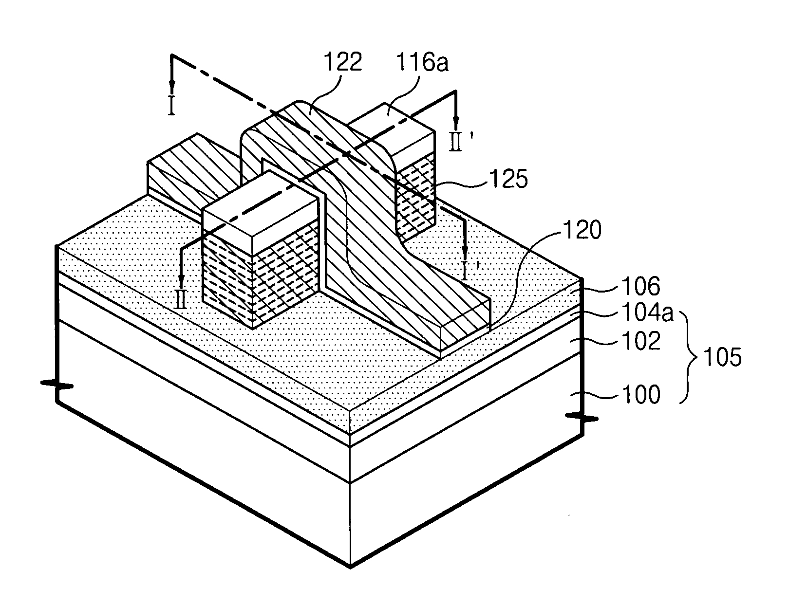
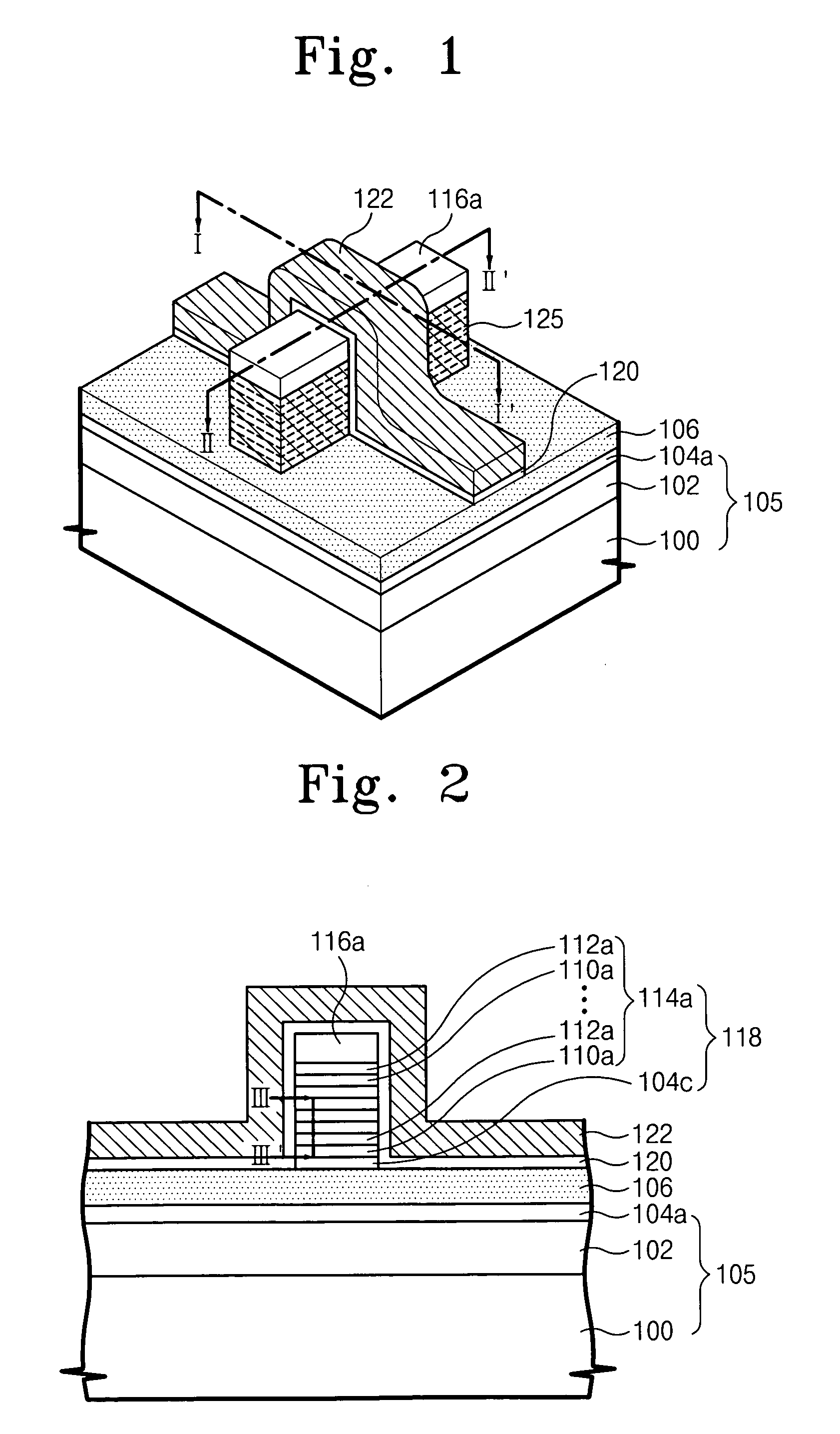
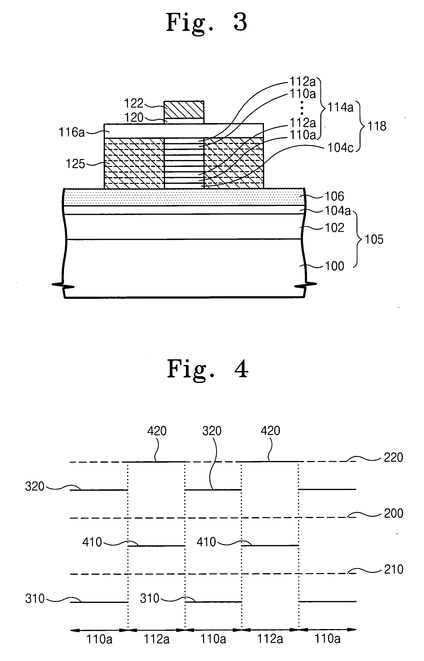
[0027] The present invention now will be described more fully hereinafter with reference to the accompanying drawings, in which preferred embodiments of the invention are shown. This invention may, however, be embodied in many different forms and should not be construed as limited to the embodiments set forth herein; rather, these embodiments are provided so that this disclosure will be thorough and complete, and will fully convey the scope of the invention to those skilled in the art. In the drawings, the thicknesses of layers and regions are exaggerated for clarity. It will be understood that when an element such as a layer, region or substrate is referred to as being “on” another element, it can be directly on the other element or intervening elements may also be present. It will be understood that when an element such as a layer, region or substrate is referred to as “under” another element, it can be directly under the other element or intervening elements may also be present. ...


PUM


Abstract

A fin field effect transistor has a fin pattern protruding from a semiconductor substrate. The fin pattern includes first semiconductor patterns and second semiconductor patterns which are stacked. The first and second semiconductor patterns have lattice widths that are greater than a lattice width of the substrate in at least one direction. In addition, the first and second semiconductor patterns may be alternately stacked to increase the height of the fin pattern, such that one of the first and second patterns can reduce stress from the other of the first and second patterns. The first and second semiconductor patterns may be formed of strained silicon and silicon-germanium, where the silicon-germanium patterns can reduce stress from the strained silicon patterns. Therefore, both the number of carriers and the mobility of carriers in the transistor channel may be increased, improving performance of the fin field effect transistor. Related methods are also discussed.

Description

CROSS REFERENCE TO RELATED APPLICATION [0001] This application claims priority under 35 U.S.C. § 119 from Korean Patent Application No. 2003-50569, filed Jul. 23, 2003, the contents of which are incorporated herein by reference in their entirety. FIELD OF THE INVENTION [0002] The present invention generally relates to semiconductor integrated circuit devices, and more specifically, to fin field effect transistors and methods of forming the same. BACKGROUND OF THE INVENTION [0003] Field effect transistors are employed as basic discrete elements in fabricating semiconductor integrated circuit devices. Generally, a field effect transistor is composed of a gate electrode, a source region, and a drain region. The source and drain regions are located in a semiconductor substrate, with the source region separated from the drain region. The gate electrode is positioned over a channel region between the source and the drain regions. In the following specification, ‘field effect transistor’ w...

Claims


Application Information

Patent Timeline
Patent Type & Authority Applications(United States)
IPC IPC(8): H01L21/336H01L29/745H01L29/76H01L29/78H01L29/786
CPCH01L29/66795H01L29/78687H01L29/785H01L21/18
Inventor KIM, YOUNG-PILLEE, SUN-GHILCHOI, SI-YOUNG
Owner SAMSUNG ELECTRONICS CO LTD
Why Eureka
Try Eureka