Three-dimensional mounting structure and method for producing the same

a three-dimensional mounting and mounting structure technology, applied in the direction of printed circuit manufacturing, printed circuit non-printed electric components association, printed circuit aspects, etc., can solve the problems of increasing the development cost and the time required for designing and development, and affecting the delivery of products. , to achieve the effect of reducing the mounting area and facilitating testing

Inactive Publication Date: 2005-08-25
PANASONIC CORP
View PDF0 Cites 18 Cited by
  • Summary
  • Abstract
  • Description
  • Claims
  • Application Information

AI Technical Summary

Benefits of technology

[0009] In order to solve the above-described problems, the present invention provides a three-dimensional mounting structure that can realize high-density, multi-function mounting, can facilitate testing, as well as repair and exchange of various elements, and can reduce the mounting area, and a method for producing the same.

Problems solved by technology

On the other hand, there also is a significant disadvantage in terms of the cost or the time required for designing and development.
That is, all the necessary components may not need to be formed as a semiconductor integrated circuit, and moreover, if designing and development are carried out every time the version of a product is upgraded, an increase of the development cost and a delay of delivery of the product tend to occur.
However, in order to apply these techniques to the entire system, the same problems as those encountered in the SIP technology may occur.
However, it is more difficult to produce a multilayer configuration of wiring boards on which electronic components are mounted (as in the configurations disclosed in the above-described patent references) than commonly used wiring boards (printed circuit boards) on which electronic components are mounted two-dimensionally, thus increasing the manufacturing cost.
Nevertheless, this is problematic in terms of the manufacturing cost and the throughput.
Furthermore, among the techniques disclosed in the above-described patent references, in the case of the technique of using through holes to provide connections between the wiring boards, the wiring boards only can be tested in the stacked state, presenting the problem that defects cannot be repaired after the product has been completed.
On the other hand, in the case of using a connector to provide connection, repair and exchange are possible, but the connector and its mounting space consume a large space.
Therefore, considering the disadvantage caused by an increased mounting area, no significant effect can be achieved.

Method used


Image

  • Three-dimensional mounting structure and method for producing the same
  • Three-dimensional mounting structure and method for producing the same
  • Three-dimensional mounting structure and method for producing the same

Examples


embodiment 1

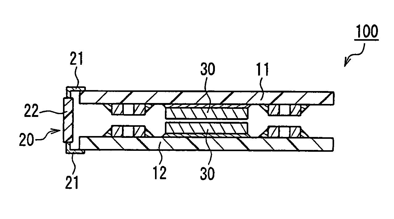
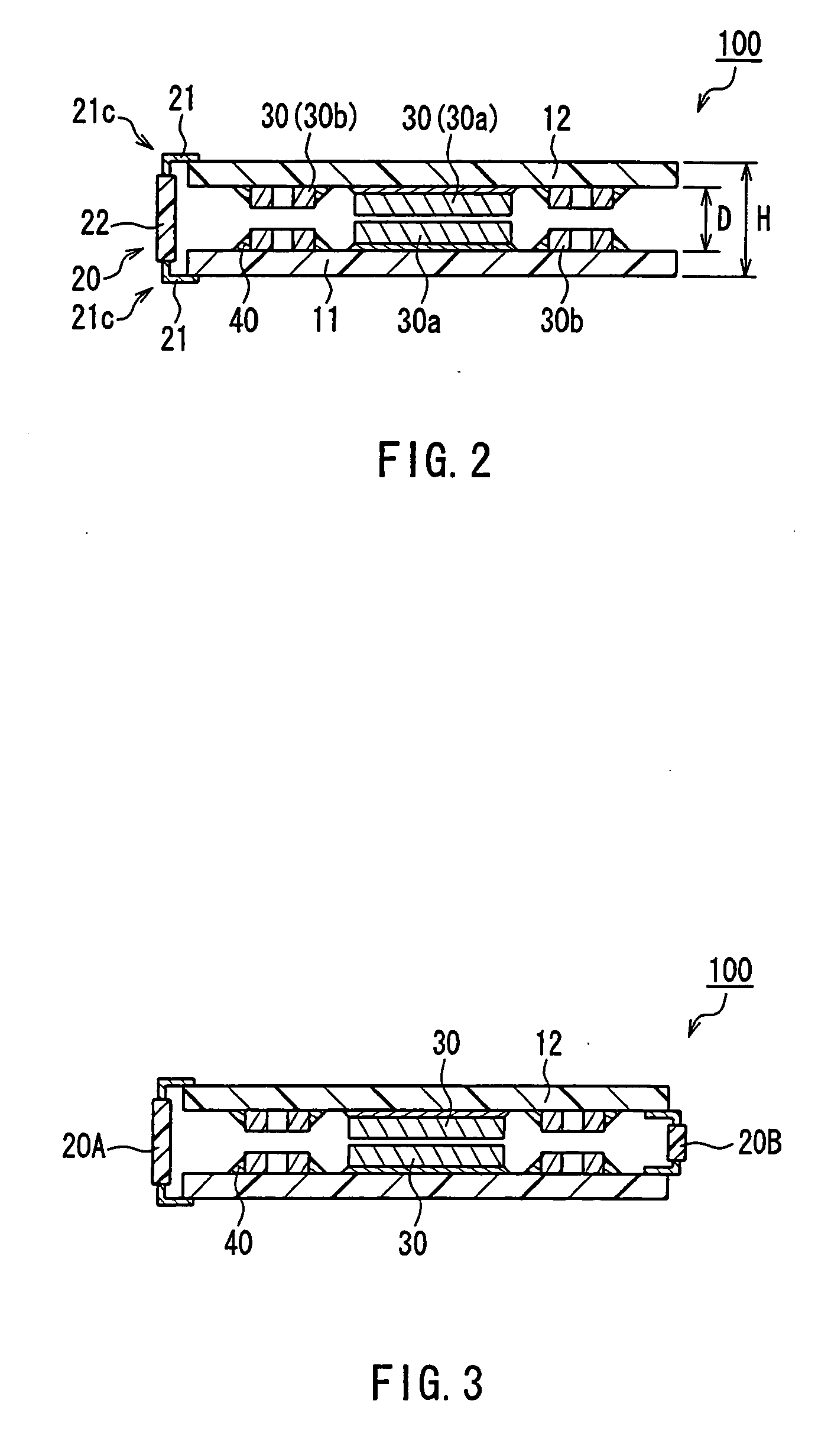
[0088] A three-dimensional mounting structure 100 according to Embodiment 1 of the present invention is described with reference to FIG. 2.

[0089] The three-dimensional mounting structure 100 shown in FIG. 2 includes: a first main wiring board 11; a second main wiring board 12 disposed substantially parallel to the first main wiring board 11; and a lead frame connector 20 disposed substantially perpendicular to the first main wiring board 11 and the second main wiring board 12. The first main wiring board 11 has a wiring pattern (not shown) on its surface, and electronic components 30 (30a, 30b) are mounted on the wiring pattern. Similarly to the first main wiring board 11, the second main wiring board 12 also has a wiring pattern (not shown) on its surface, and the electronic components 30 (30a, 30b) are mounted also on the wiring pattern of the second main wiring board 12. Examples of the electronic components 30 include a semiconductor device (e.g., a CSP and a bare chip) 30a and...

embodiment 2

[0133] In the following, a three-dimensional mounting structure according to Embodiment 2 of the present invention is described with reference to FIGS. 16 to 21. The three-dimensional mounting structure of this embodiment is an improvement or a modification of the configuration of Embodiment 1 described above. For the sake of simplicity, the description of aspects similar to those of the configuration of Embodiment 1 described above has been omitted.

[0134]FIG. 16 is a perspective view of a lead frame connector 20 whose lead wires (21a, 21b) extend in two directions. In the case of the lead frame connector 20 shown in FIG. 16, lead wires 21a that constitute a portion of the plurality of lead wires 21 extend in a substantially parallel arrangement in a first direction, and lead wires 21b that constitute the remaining portion extend in a substantially parallel arrangement in a second direction that is different from the first direction. In this embodiment, the lead wires 21a and the l...


PUM


Abstract

A three-dimensional mounting structure according to the present invention includes: a first main wiring board having a first wiring pattern on its surface and an electronic component mounted on the wiring pattern; a second main wiring board disposed facing the first main wiring board and having a second wiring pattern on its surface; and a lead frame connector disposed substantially perpendicular to the first main wiring board and the second main wiring board at an end portion of the two wiring bards, wherein the lead frame connector includes a plurality of lead wires made of an electrically conductive material and a resin portion to which the plurality of lead wires are fixed, wherein an end portion of each of the plurality of lead wires is exposed from the resin portion, and wherein at least two of the plurality of lead wires are each electrically connected to both the first wiring pattern of the first main wiring board and the second wiring pattern of the second main wiring board. Thus, there is provided a three-dimensional mounting structure that can realize high-density, multi-function mounting, allows easy testing, as well as repair and exchange of various elements and can reduce the mounting area, and a method for producing such a three-dimensional mounting structure.

Description

BACKGROUND OF THE INVENTION [0001] 1. Field of the Invention [0002] The present invention relates to three-dimensional mounting structures that are useful for, for example, mobile phones, and to methods for producing the same. In particular, the invention relates to a three-dimensional mounting structure that can realize high-density, multi-function mounting, and to a method for producing such a three-dimensional mounting structure. [0003] 2. Related Background Art [0004] With the recent miniaturization and performance enhancement of electronic devices, there is an increasing demand for the high-density mounting of electronic components mounted on printed boards and the performance enhancement of circuit boards on which the electronic components are mounted. Under such circumstances, extensive research and development have been conducted on, for example, system-on-chip (SOC) technology that realizes high-density, multi-function mounting with the use of system LSIs in which a one-chi...

Claims


Application Information

Patent Timeline
Patent Type & Authority Applications(United States)
IPC IPC(8): H01L23/48H05K1/14H05K1/18H05K3/00H05K3/36H05K7/02
CPCH05K1/141H05K1/148H05K3/0052H05K3/36H05K2201/10424H01L2224/16225H01L2224/32225H01L2924/19105H01L2224/73204H01L2924/00
Inventor ASAHI, TOSHIYUKINAKATANI, SEIICHINISHIYAMA, TOUSAKUNAKANISHI, KIYOSHIMURAMATSU, KEN
Owner PANASONIC CORP
Why Eureka
Try Eureka