Charge trapping memory cell and fabrication method

a memory cell and charge trapping technology, applied in the field of semiconductor device methods, can solve the problems of restricted storage medium, achieve the effects of weaker electric fields, small area, and improved programming and erasing properties

Inactive Publication Date: 2005-09-01
POLARIS INNOVATIONS
View PDF14 Cites 29 Cited by
  • Summary
  • Abstract
  • Description
  • Claims
  • Application Information

AI Technical Summary

Benefits of technology

[0008] In one aspect, the present invention specifies a charge trapping memory cell that has improved programming and erasing properties in conjunction with a small area requirement, and an associated fabrication method.
[0009] The memory cell according to the preferred embodiment of the invention involves forming a charge trapping memory cell with the structure of a trench transistor, two gate electrodes electrically insulated from one another being provided in the trench in order to enable programming by source-side injection. This programming mechanism manages with weaker electric fields, lower electric field strengths occurring in particular in the region of the curvature of the channel at the bottom of the trench. Moreover, in preferred configurations, the storage medium is restricted to a narrowly delimited region. This significantly reduces disturbing effects such as, by way of example, the influencing of a second bit stored in the same cell. The arrangement in the trench ensures a small area requirement of the memory cell. The high field strengths are limited to the actual storage region by the programming mechanism of source-side injection. The two gate electrodes arranged in the trench are electrically insulated from one another by a layer made of dielectric material that is coplanar with respect to the top side of the semiconductor body. The bottom gate electrodes respectively present in a relevant trench are continuously electrically interconnected and contact-connected on the top side at the edge of the memory cell array. The top gate electrodes are connected in a manner known per se by means of word lines running transversely with respect to the trenches. The source / drain regions formed between the trenches at the top side of the semiconductor body by implantation of dopant are interconnected in the longitudinal direction of the trenches by buried bit lines formed in the semiconductor material.

Problems solved by technology

Moreover, in preferred configurations, the storage medium is restricted to a narrowly delimited region.

Method used


Image

  • Charge trapping memory cell and fabrication method
  • Charge trapping memory cell and fabrication method
  • Charge trapping memory cell and fabrication method

Examples


Embodiment Construction

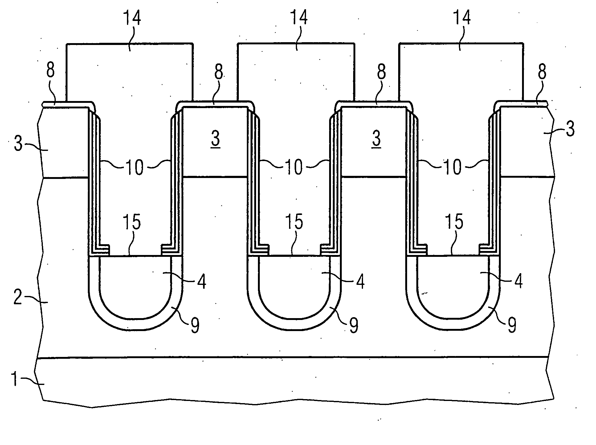
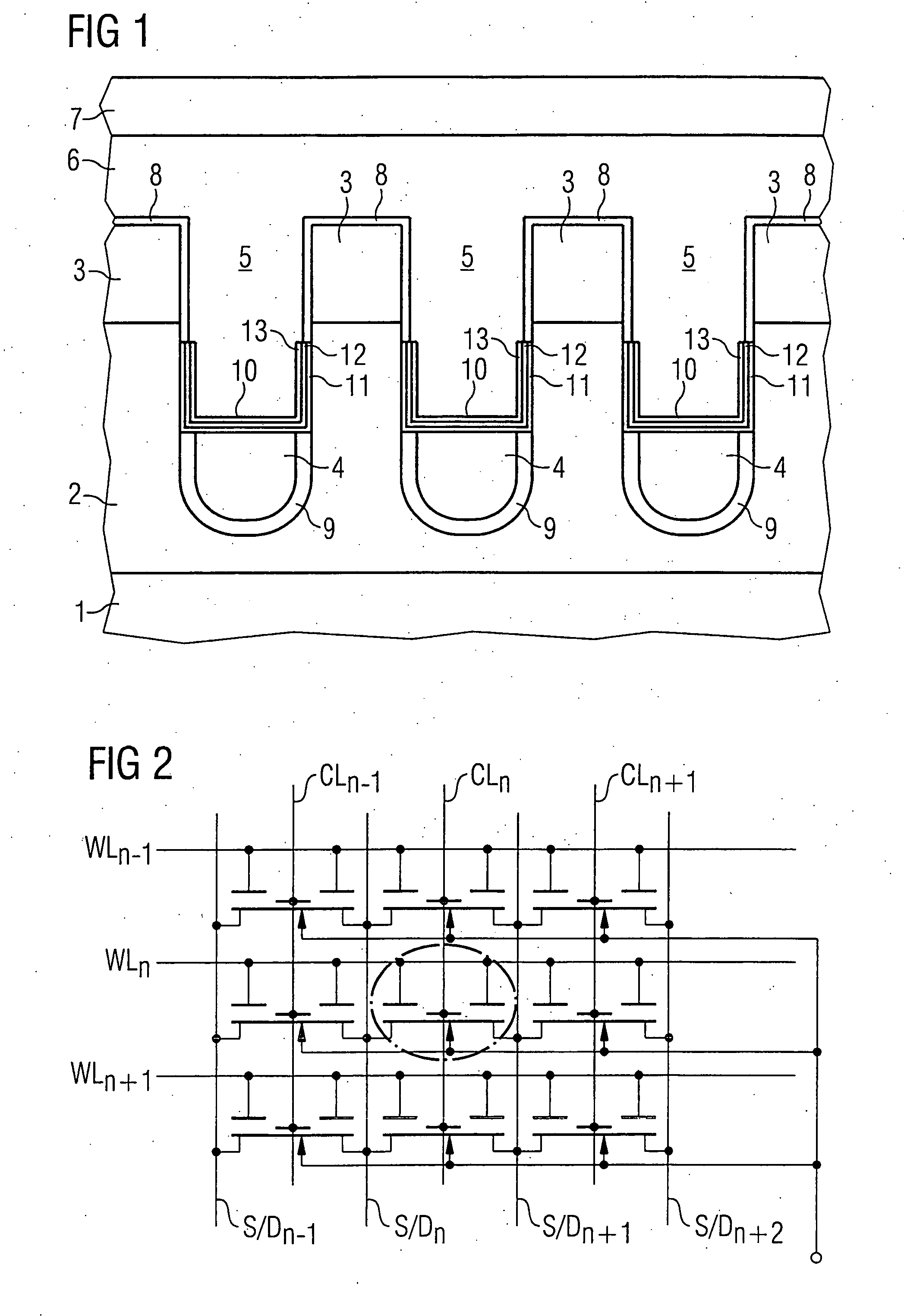
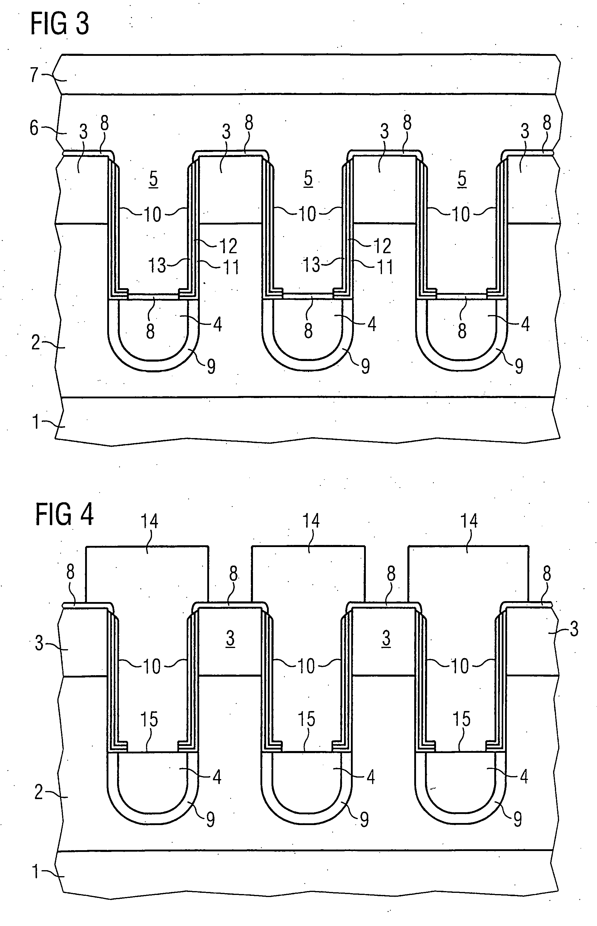
[0041]FIG. 1 shows a detail from a cross section through a memory cell array formed with the charge trapping memory cells. A doped well 2, preferably p-conducting, is fabricated in a semiconductor body 1, such as a substrate or a semiconductor layer grown on a substrate. Trenches are situated in the well, the transistor structures of the memory cells being formed in the trenches. At the top side of the semiconductor body 1, source / drain regions 3 doped opposite to the conductivity type of the well 2 are situated between the trenches and in a manner adjoining the latter. Situated in the lower region of the trenches are first gate electrodes 4, which are in each case insulated from the semiconductor material of the doped well 2 by a gate dielectric 9. The trenches are formed with curved bottoms, and the entire curved region is covered by the first gate electrodes 4. Second gate electrodes 5 are situated above the first gate electrodes 4 in the trenches. The first gate electrodes and t...


PUM


Abstract

A memory cell patterned as a trench transistor is provided with a first gate electrode (4) as auxiliary gate for source-side injection and a second gate electrode (5) electrically insulated therefrom, which are arranged in the trench, and has, at the trench walls, a storage layer sequence (10) provided for charge trapping and comprising a storage layer (12) between boundary layers (11, 13). The first gate electrode (4) and the second gate electrode (5) are electrically insulated from one another, which can be effected by means of a portion of the storage layer sequence (10). Source/drain regions (3) are arranged on the top side laterally with respect to the trenches. Word lines (6), source/drain lines and control gate lines are present for the electrical driving.

Description

[0001] This application claims priority to German Patent Application 10 2004 006505.5, which was filed Feb. 10, 2005, and is incorporated herein by reference. TECHNICAL FIELD [0002] The present invention relates generally to semiconductor devices methods, and more particularly to a charge trapping memory cell and fabrication method. BACKGROUND [0003] In charge trapping memory cells, which are nonvolatile memory cells based on charge storage between the channel region and / or the source / drain regions and the gate electrode, as part of the gate dielectric, a nonconductive storage layer is present between boundary layers for trapping charge carriers and thus for altering the programming state of the memory cell. Examples thereof include SONOS memory cells (semiconductor-oxide-nitride-oxide-semiconductor; see U.S. Pat. No. 5,768,192, U.S. Pat. No. 6,011,725, PCT Publication WO 99 / 60631), in which each boundary layer is an oxide and the storage layer is a nitride of the semiconductor mate...

Claims


Application Information

Patent Timeline
Patent Type & Authority Applications(United States)
IPC IPC(8): H01L21/8238H01L21/8246H01L21/8247H01L27/115H01L29/76
CPCH01L27/11568H01L27/115H10B69/00H10B43/30
Inventor MIKOLAJICK, THOMAS
Owner POLARIS INNOVATIONS
Why Eureka
Try Eureka