Organic electroluminescent display device and method of fabricating the same

a technology of electroluminescent display device and electroluminescent light, which is applied in the direction of radiation control device, identification means, instruments, etc., can solve the problems of preventing use of large-area displays, power consumption, and low power consumption of electroluminescent display devices, so as to improve yield and productivity

Inactive Publication Date: 2005-09-01
LG DISPLAY CO LTD
View PDF4 Cites 8 Cited by
  • Summary
  • Abstract
  • Description
  • Claims
  • Application Information

AI Technical Summary

Benefits of technology

[0018] Another object of the present invention is to provide an organic electro-luminescent display device and a method of fabricating the same having an improved yield and productivity.
[0019] Another object of the present invention is to provide an organic electro-luminescent display device and a method of fabricating the same that are reliable.

Problems solved by technology

The organic electroluminescent display device also has low power consumption, high brightness, and short response time.
However, the passive matrix-type organic electroluminescent display devices have high power consumption, thereby preventing use in large area displays.
The yield of the AMOELD device varies due to impurities in the process of forming the organic layer to a thickness of about 1,000 Å. Accordingly, the yield of the AMOELD is reduced because of the impurities, thereby resulting in a loss of manufacturing costs and source materials for the thin film transistor.
However, the bottom emission mode device has a reduced aperture ratio.
Thus, the bottom emission mode AMOELD has difficulty in being used as a high aperture device.
However, in the top emission mode AMOELD, since a cathode electrode is generally disposed over the organic layer, a choice of material with which to make the cathode electrode is limited.
Accordingly, transmittance of light is limited, and a luminous efficacy is reduced.

Method used


Image

  • Organic electroluminescent display device and method of fabricating the same
  • Organic electroluminescent display device and method of fabricating the same
  • Organic electroluminescent display device and method of fabricating the same

Examples


Embodiment Construction

[0034] Reference will now be made in detail to the illustrated embodiment of the present invention, an example of which is illustrated in the accompanying drawings.

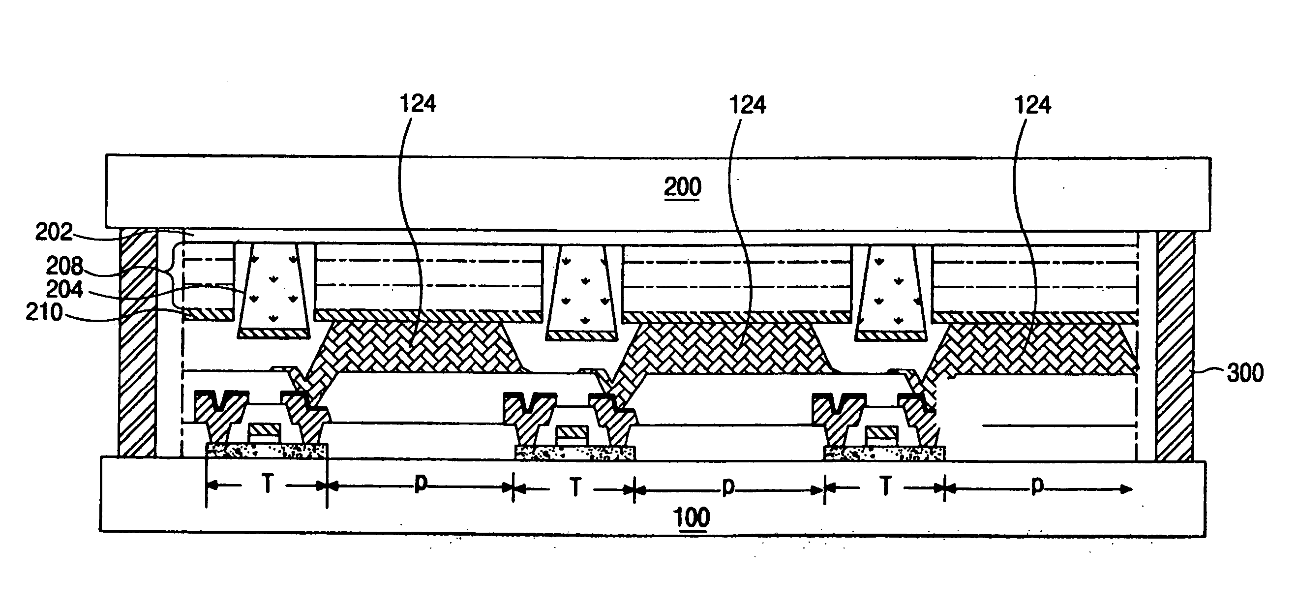
[0035]FIG. 5 is a cross sectional view of an exemplary AMOELD device according to the present invention. In FIG. 5, the AMOELD device may include a first substrate 100 and a second substrate 200 that are spaced apart and face each other. A sealant 300 may be formed between the first and second substrates 100 and 200 to bond the first and second substrates 100 and 200 together.

[0036] A plurality of thin film transistors T may be formed on an inner surface of the first substrate 100, wherein the thin film transistor T may functions as a driving thin film transistor of the AMOELD device. Although not shown, a switching thin film transistor, a gate line, a data line, and a power line may also formed on the inner surface of the first substrate 100.

[0037] A first electrode 202 may be formed on an inner surface of the second ...


PUM


Abstract

An organic electroluminescent display device includes a first substrate, a second substrate spaced apart and facing the first substrate, a switching thin film transistor disposed on an inner surface of the first substrate, a driving thin film transistor electrically connected to the switching thin film transistor, a connecting electrode electrically connected to the driving thin film transistor, a first electrode disposed on an inner surface of the second substrate, a partition wall disposed on the first electrode and having a transmissive hole corresponding to a pixel region between the first and second substrates, an organic layer disposed within the transmissive hole on the first electrode, and a second electrode disposed on the organic layer, wherein the second electrode is electrically connected to the driving thin film transistor through the connecting electrode.

Description

[0001] This application is a Continuation of Copending U.S. patent application Ser. No. 10 / 328,923 and claims the benefit of the Korean Patent Application No. P2002-024552 filed in Korea on May 3, 2002, which are hereby incorporated by reference in their entirety.BACKGROUND OF THE INVENTION [0002] 1. Field of the Invention [0003] The present invention relates to an electroluminescent display device, and more particularly, to an organic electroluminescent display device and a method of fabricating the same. [0004] 2. Discussion of the Related Art [0005] In general, an organic electroluminescent display device emits light by injecting electrons from a cathode electrode and holes from an anode electrode into an emissive layer, combining the electrons and the holes to generate an exciton, and transiting the exciton from an excited state to a ground state. Since the organic electroluminescent display device does not require an additional light source due to its self-luminescence, the org...

Claims


Application Information

Patent Timeline
Patent Type & Authority Applications(United States)
IPC IPC(8): G09F9/30H01L27/32H01L51/50H01L51/52H05B33/10H05B33/12H05B33/22
CPCH01L27/3246H01L27/3251H01L2251/5315H01L51/5237H01L27/3253H10K59/122H10K59/127H10K59/1275H10K2102/3026H05B33/22H10K50/841
Inventor PARK, JAE-YONGYOO, CHOONG-KEUNKIM, OCK-HEELEE, NAM-YANGKIM, KWAN-SOO
Owner LG DISPLAY CO LTD
Why Eureka
Try Eureka