Ogs touch screen substrate and method of manufacturing the same, and related apparatus

Active Publication Date: 2016-09-01
BOE TECH GRP CO LTD
View PDF1 Cites 4 Cited by
  • Summary
  • Abstract
  • Description
  • Claims
  • Application Information

AI Technical Summary

Benefits of technology

The present invention provides a touch screen substrate and a method of manufacturing it that simplifies the manufacturing process and increases yield. The method utilizes different chemical properties of copper, nanoscale silver, and ITO materials to create electrical connection lines and conductive bridges. This improves productivity and yield, and the nanoscale silver has lower resistance than ITO, making it ideal for large-size touch-sensitive OGS panels.

Problems solved by technology

Thus, the conventional process of manufacturing a touch screen substrate becomes complex and thus leads to a rather low yield.

Method used


Image

  • Ogs touch screen substrate and method of manufacturing the same, and related apparatus
  • Ogs touch screen substrate and method of manufacturing the same, and related apparatus
  • Ogs touch screen substrate and method of manufacturing the same, and related apparatus

Examples


Embodiment Construction

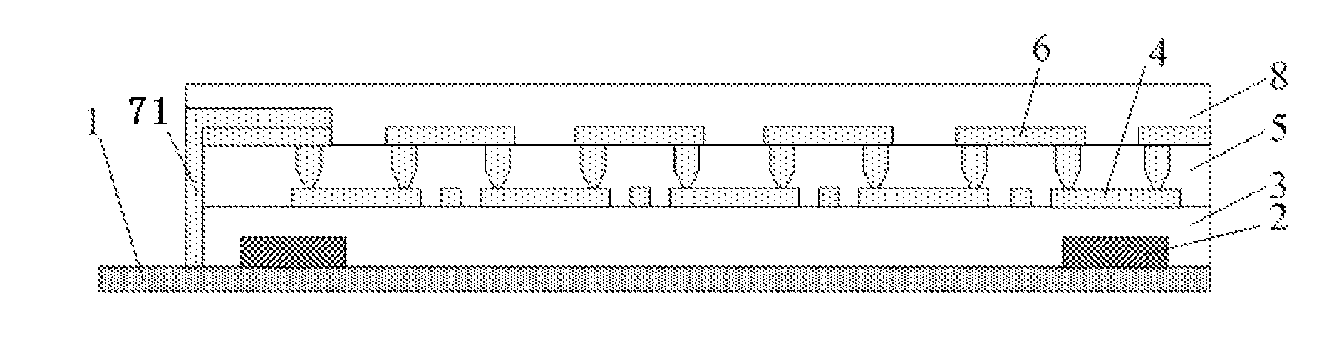
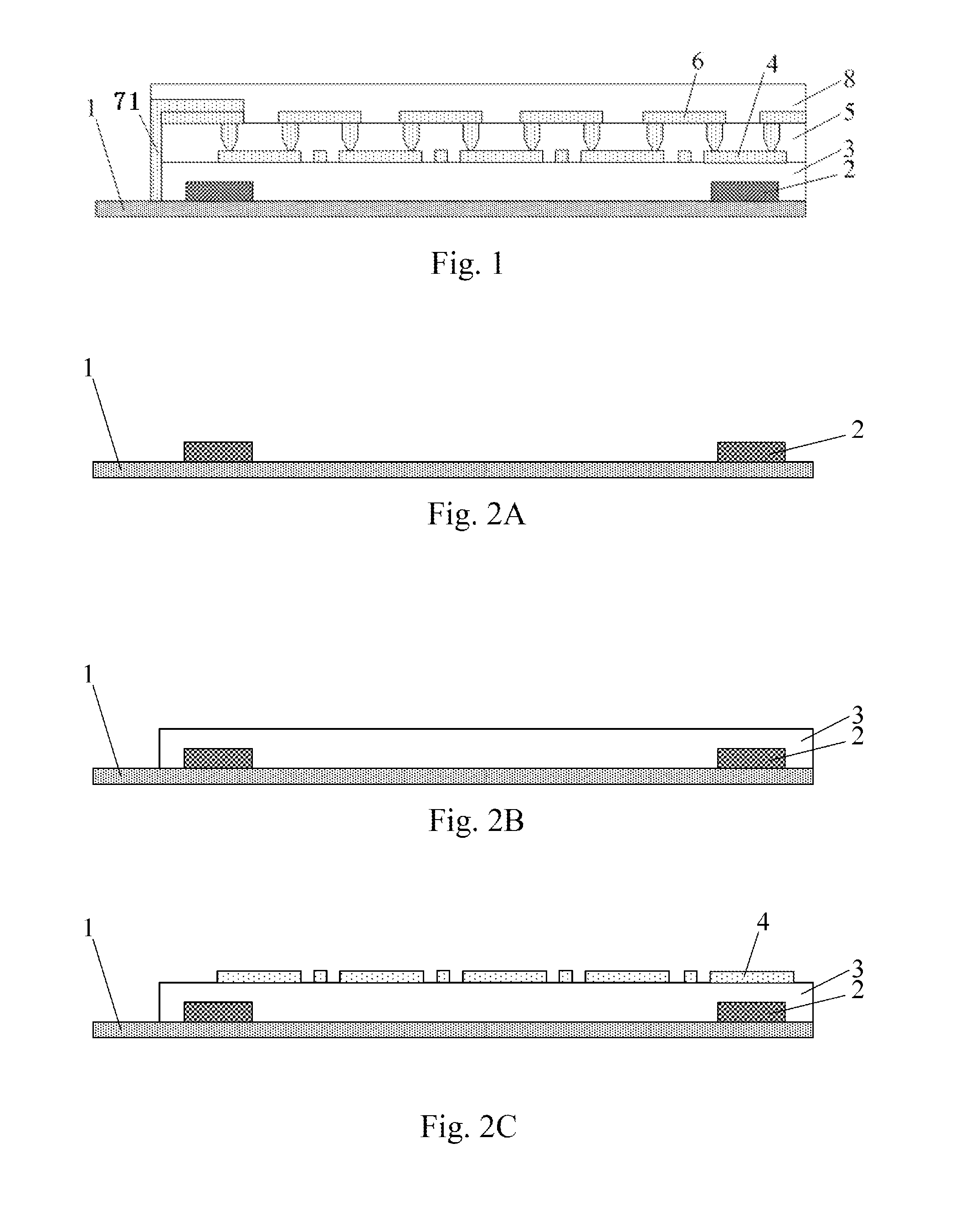
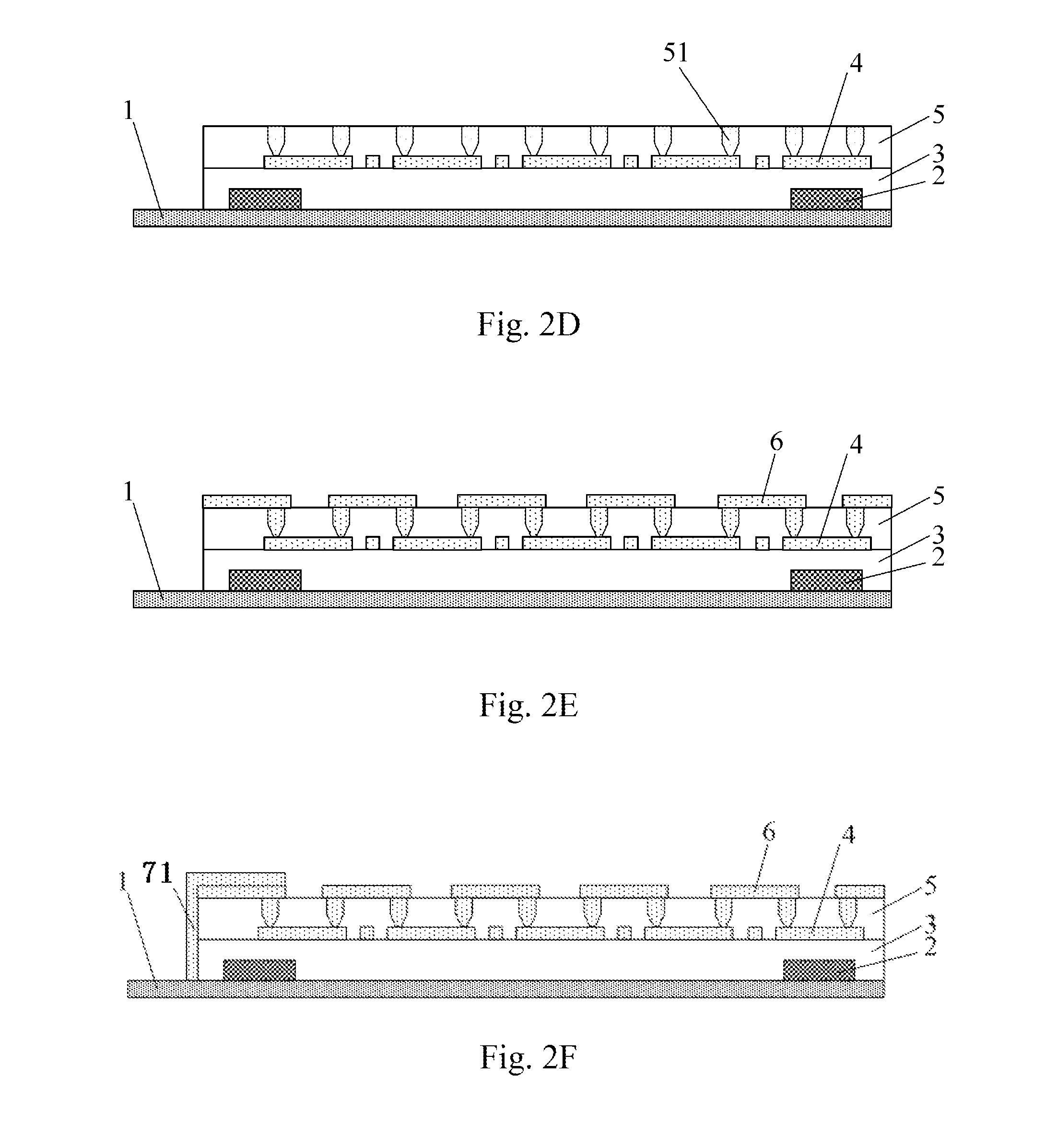
[0036]According to the present invention, it is proposed that a capacitance layer is made of nanoscale silver, and through holes and conductive bridges are made of nanoscale silver or ITO while electrical connection lines are made of a different material, for example, copper. As the conductive bridges and the electrical connection lines are designed to be made of different materials, they may be formed through an ashing and etching process, thereby simplifying the process.

[0037]In order to make the object, technical solutions and advantages of the present invention more clear, the embodiments of the present invention are illustrated and described in detailed by reference to the accompanying drawings.

[0038]FIG. 3 is a side sectional view of a touch screen substrate of an embodiment of the present invention. As shown in FIG. 3, the touch screen substrate includes a capacitance layer including a plurality of electrodes; a first cover layer 5 formed on the capacitance layer; a plurality...


PUM


Abstract

The present invention discloses a touch screen substrate and a method of manufacturing the same. The touch screen substrate includes a capacitance layer comprising a plurality of electrodes, a first cover layer formed on the capacitance layer; a plurality of conductive bridges located on the first cover layer and configured to be electrically connected to a part of the electrodes that are electrically isolated; and a plurality of electrical connection lines, configured to respectively be electrically connected to the respective conductive bridge so as to electrically connect the first electrode with a touch detecting circuit. A material layer for forming the electrical connection lines is different from a material layer for forming the conductive bridges such that the conductive bridges located below the electrical connection lines are not corroded when the material layer for the electrical connection lines is etched. Utilization of different chemical properties of copper and silver nanowires and ITO material and inclusion of a single patterning process increase productivity and yield.

Description

BACKGROUND[0001]1. Technical Field[0002]The present invention relates to the field of touch screen, and particularly to an OGS touch screen substrate, a method of manufacturing a touch screen substrate, a display apparatus including a touch screen, and more particularly to a process of forming a capacitance layer by silver nanowires and of forming bridges by copper.[0003]2. Description of the Related Art[0004]A touch screen, serving as a smart man-machine interface product, has been applied widely in many applications of daily life and production, particularly in consumer electronics products (such as, smart mobile phone, tablet, etc.).[0005]The touch screen mainly includes resistance type, capacitance type, infrared type and surface acoustic type touch screens. A capacitance type touch screen has advantages of rapid response, multi-touch and long lifetime and thus becomes current main technology in market.[0006]An OGS (One Glass Solution) capacitance touch screen has advantages of ...

Claims


Application Information

Patent Timeline
IPC IPC(8): G06F3/044
CPCG06F2203/04103G06F3/044G06F3/0443G06F3/0446
Inventor YAO, QIZHANG, FENGCAO, ZHANFENGLIU, ZHENHE, XIAOLONG
Owner BOE TECH GRP CO LTD
Why Eureka
Try Eureka