Semiconductor device and method of the semiconductor device

Inactive Publication Date: 2005-06-28
HITACHI LTD +1
View PDF8 Cites 17 Cited by
  • Summary
  • Abstract
  • Description
  • Claims
  • Application Information

AI Technical Summary

Benefits of technology

[0008]Another object of the present invention is to provide a semiconductor integrated circuit device which improves the productivity and yield of products, and facilitates the production management.
[0009]Still another object of the present invention is to provide a method of manufacturing semiconductor integrated circuit devices which enables the enhancement of productivity and yield of products and the rational demand-responsive production management.

Problems solved by technology

For example, integrated circuit devices used in personal computer systems operate at such a relatively high voltage as 3.0 V, those used in portable terminal units operate at such an intermediate voltage as 2.5 V, and those mounted on IC cards operate at such a low voltage as 1.8 V. Due to different types of semiconductor integrated circuit devices, which are identical in internal memory structure but different in operating voltage, the production efficiency is deteriorated.

Method used


Image

  • Semiconductor device and method of the semiconductor device
  • Semiconductor device and method of the semiconductor device
  • Semiconductor device and method of the semiconductor device

Examples


Embodiment Construction

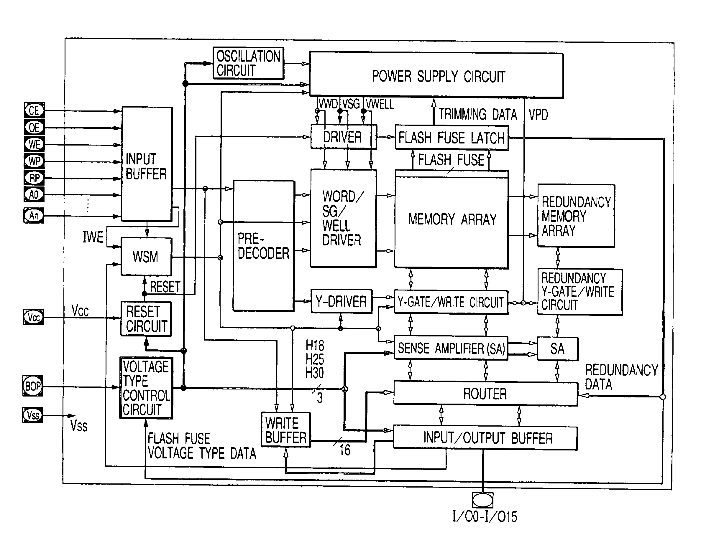
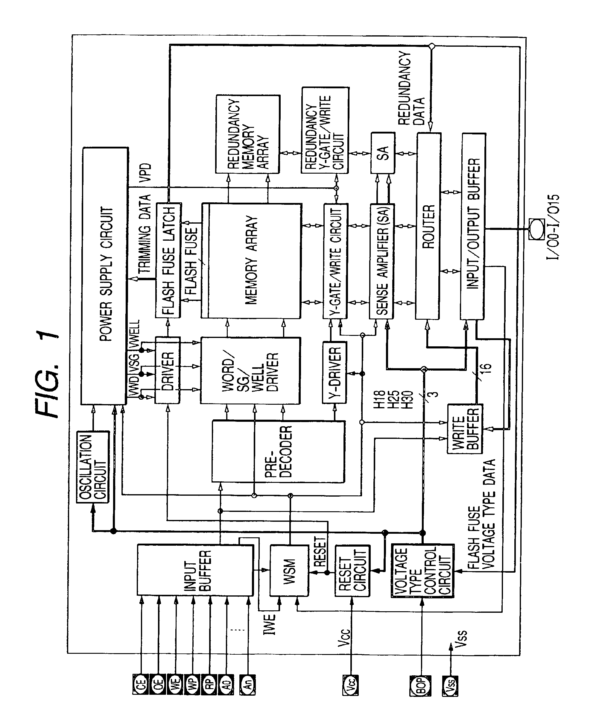
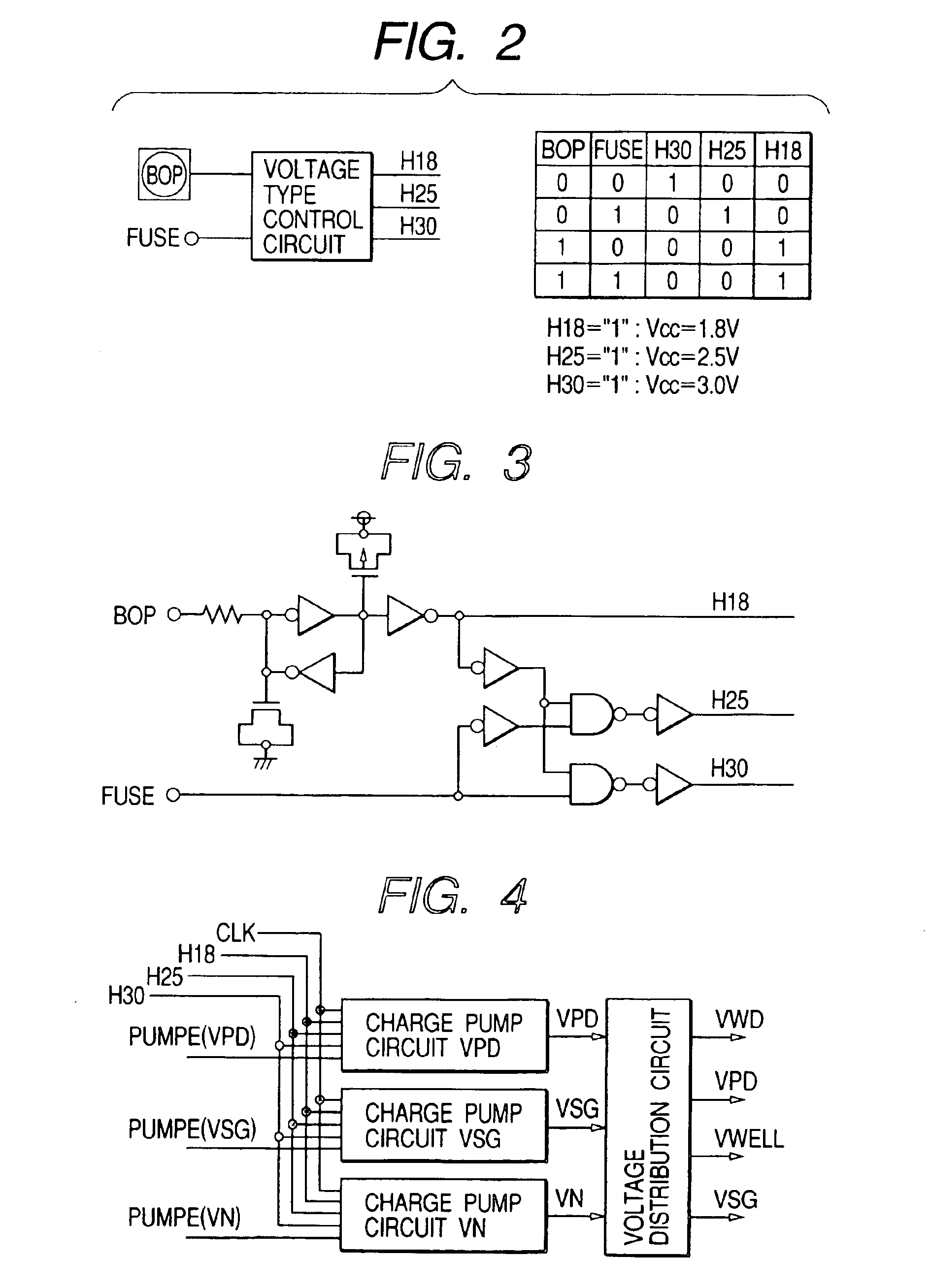
[0049]FIG. 1 shows by block diagram the overall arrangement of the nonvolatile memory based on an embodiment of this invention. The circuit blocks shown in the figure are formed by the known semiconductor integrated circuit fabrication process on a semiconductor substrate of monocrystalline silicon for example.

[0050]The memory array is nonvolatile memory cells, each having a control gate and floating gate in a stacked gate structure, arranged on the intersections of the matrix of word lines and data lines. Each memory cell has its control gate electrode, drain electrode and source electrode connected to a word line, data line and source line, respectively. The write operation of memory cell is based on the tunnel current flowing through the thin oxide film, or based on hot electrons created by the current flowing between the source and drain, although this affair is not compulsory. The erase operation of memory cell is based on the tunnel current. The redundancy memory array include...


PUM


Abstract

Disclosed are a semiconductor chip which is uniquely value-added, a semiconductor integrated circuit device which improves the productivity and yield of products and facilitates the production management, and a method of manufacturing of semiconductor integrated circuit devices which enables the improvement of productivity and yield of products and the rational demand-responsive production management. The semiconductor chip includes a common circuit block which is operative at a first voltage and a second voltage that is higher than the first voltage, a first circuit block which is designed to fit the first voltage and operate in unison with the common circuit block, a second circuit block which is designed to fit the second voltage and operate in unison with the common circuit block, and a voltage type setup circuit which activates one of the first and second circuit blocks, with a first identification record indicative of the operability at the first voltage or a second identification record indicative of the operability only at the second voltage being held by the chip.

Description

CROSS-REFERENCE TO RELATED APPLICATION[0001]This application is a continuation of application Ser. No. 10 / 132,248 filed Apr. 26, 2002 now U.S. Pat. No. 6,667,928.BACKGROUND OF THE INVENTION[0002]The present invention relates to a semiconductor chip, a semiconductor integrated circuit device, and a method of manufacturing semiconductor integrated circuit devices, and particularly to a technique useful for the manufacturing of nonvolatile memories of the type of block-erasure.[0003]EEPROM of the type of electrical block erasure is a nonvolatile memory device having a function of erasing at once all memory cells or a block of memory cells formed on a semiconductor chip. The electrically block erasing EEPROM has a memory cell structure which resembles that of ordinary EPROM. Specifically, a memory cell is formed of an insulated gate field effect transistor having a double-layer structure (will be termed “MOSFET” or simply “transistor”), which stores data virtually in terms of the variat...

Claims


Application Information

Patent Timeline
IPC IPC(8): G11C5/14G11C16/30G11C16/06G11C29/00G11C29/02G01R31/28G11C16/02G11C16/16G11C17/00G11C29/12G11C29/44
CPCG11C5/14G11C16/30G11C29/02G11C29/028G11C29/12005G11C29/006G11C16/04G11C2029/5004G11C16/16
Inventor HONMA, KAZUKIKAWAJIRI, YOSHIKIWADA, MASASHISUGAWARA, MIKIOSONOYAMA, HIROFUMI
Owner HITACHI LTD
Why Eureka
Try Eureka