Dual panel-type organic electroluminescent display device and method of fabricating the same

a display device and organic electroluminescent technology, applied in the field of display devices and methods of fabricating the same, can solve the problems of low power consumption, large viewing angle of devices and achieve the effects of improving yield and productivity, high aperture ratio, and high contrast ratio

Active Publication Date: 2008-03-04
LG DISPLAY CO LTD
View PDF17 Cites 3 Cited by
  • Summary
  • Abstract
  • Description
  • Claims
  • Application Information

AI Technical Summary

Benefits of technology

[0020]An object of the present invention is to provide a dual panel-type OELD device and a method of fabricating a dual panel-type OELD device having a high aperture ratio and producing high definition images.
[0021]Another object of the present invention is to provide a dual panel-type OELD device and a method of fabricating a dual panel-type OELD device having an improved yield and productivity.
[0022]Another object of the present invention is to provide a dual panel-type OELD device and a method of fabricating a dual panel-type OELD device having improved operational reliability.

Problems solved by technology

In addition, OELD devices have wide viewing angles and high contrast ratios, and are relatively small and lightweight, as compared to a liquid crystal display (LCD) devices and plasma display panel (PDP) devices.
Moreover, OELD devices have low power consumption, and are commonly driven by low direct current (DC) voltages, thereby providing relatively short response times. Since OELD devices are solid state, they can operate within a wide range of temperatures, and are unlikely to be damaged by external impacts.
Thus, even though the array elements may be properly fabricated, if the organic light-emitting layer is improperly fabricated, such forming the layer having a thickness of about 1,000 Å or incorporating impurities or other factors, the resulting OELD device will be determined to be unacceptable.
Thus, all manufacturing costs and source materials required for fabrication of the array elements are wasted, and product yield is lowered.
Thus, the bottom emission mode OELD device is not generally suitable for a high aperture device.
Conversely, a top emission mode OELD device has a high aperture ratio, is easy to fabricate, and has a long operational lifetime.
However, in the top emission mode OELD device, since a cathode is generally disposed over the organic light-emitting layer, a choice of material with which to make the cathode is limited.
Accordingly, light transmittance is limited, and light-emitting efficacy is reduced.

Method used


Image

  • Dual panel-type organic electroluminescent display device and method of fabricating the same
  • Dual panel-type organic electroluminescent display device and method of fabricating the same
  • Dual panel-type organic electroluminescent display device and method of fabricating the same

Examples


Embodiment Construction

[0035]Reference will now be made in detail to the preferred embodiments of the present invention, examples of which are illustrated in the accompanying drawings.

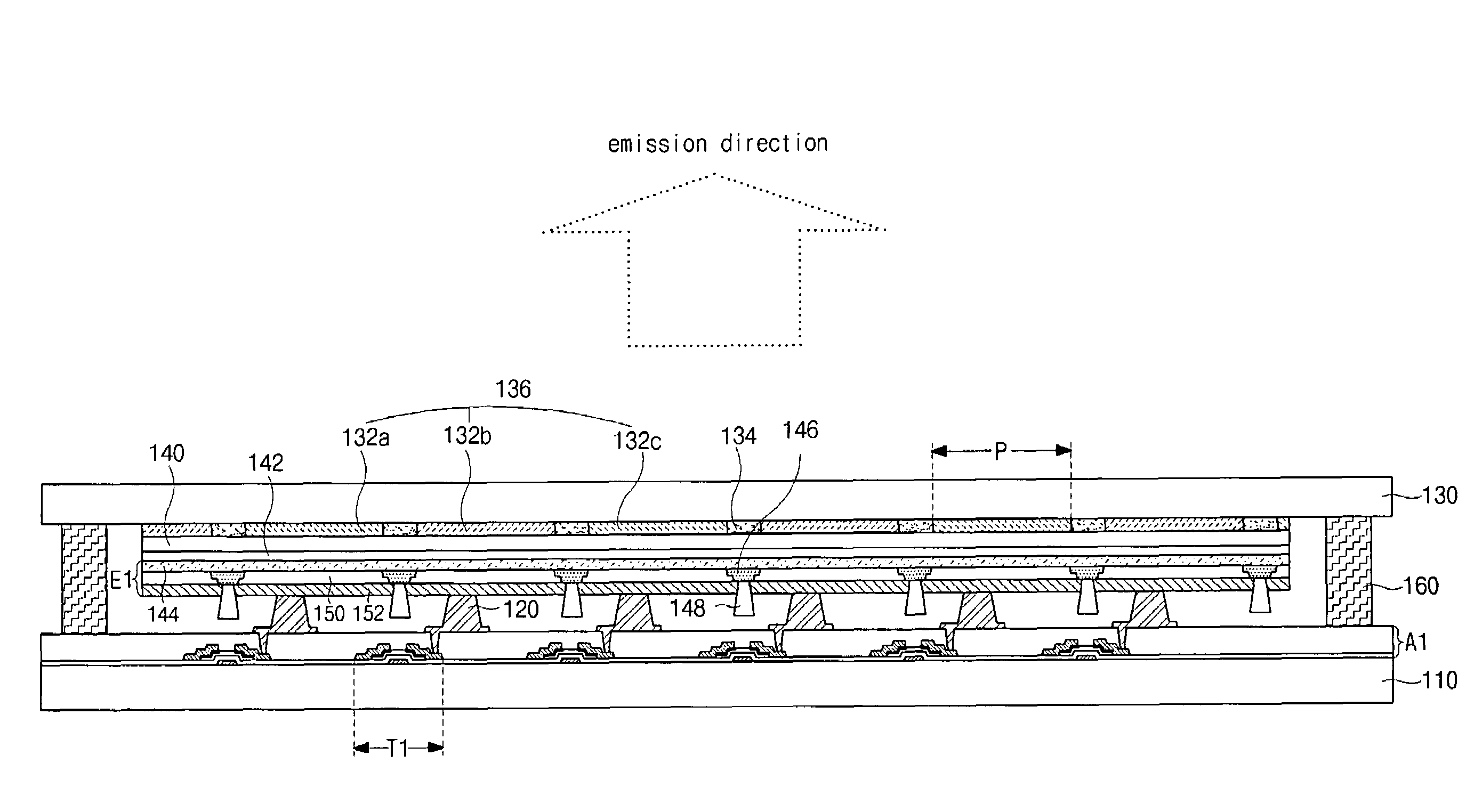
[0036]FIG. 3 is a cross sectional view of an exemplary dual panel-type OELD device according to the present invention. In FIG. 3, a dual panel-type OELD device may include a first substrate 110 and a second substrate 130 that are spaced apart and face each other. In addition, an array element layer A1 including a plurality of thin film transistors T1 may be formed on an inner surface of the first substrate 110, wherein a plurality of connection patterns 120 having a predetermined thickness may be formed on the array element layer A1. Accordingly, each connection pattern 120 may be connected to each thin film transistor T1. Although not shown, the array element layer A1 may further includes gate lines, data lines, power lines, and switching thin film transistors.

[0037]The connection patterns 120 may be formed of an organic in...


PUM


Abstract

A dual panel-type organic electroluminescent display device includes first and second substrates facing and spaced apart from each other, an array element layer disposed along an inner surface of the first substrate, the array element including a thin film transistor, a connection pattern disposed on the array element layer and electrically connected to the thin film transistor, a color filter layer disposed along an inner surface of the second substrate, the color filter layer including red, green, and blue color filters, an overcoat layer disposed on the color filter layer, the overcoat layer including a hygroscopic material, an organic electroluminescent diode disposed on the overcoat layer and connected to the connection pattern, the organic electroluminescent diode including a first electrode, an organic light-emitting layer, and a second electrode sequentially formed on the overcoat layer, and the organic light-emitting layer emits substantially monochromatic light, and a seal pattern along peripheral portions between the first and second substrates.

Description

[0001]The present invention claims the benefit of Korean Patent Application No. P2003-0097880 filed in Korea on Dec. 26, 2003, which is hereby incorporated by reference.BACKGROUND OF THE INVENTION[0002]1. Field of the Invention[0003]The present invention relates to a display device and a method of fabricating a display device, and more particularly, to a dual panel-type OELD device and a method of fabricating a dual panel-type OELD device.[0004]2. Discussion of the Related Art[0005]Presently, OELD devices are self-luminescent and do not require additional light sources. In addition, OELD devices have wide viewing angles and high contrast ratios, and are relatively small and lightweight, as compared to a liquid crystal display (LCD) devices and plasma display panel (PDP) devices. Moreover, OELD devices have low power consumption, and are commonly driven by low direct current (DC) voltages, thereby providing relatively short response times. Since OELD devices are solid state, they can...

Claims


Application Information

Patent Timeline
Patent Type & Authority Patents(United States)
IPC IPC(8): H01L29/04H05B33/04H01L21/00H01L27/32H01L29/08H01L35/24H01L51/52H05B33/02H05B33/10H05B33/12H05B33/22H05B33/26
CPCH01L27/322H01L27/3251H01L51/5237H01L51/5284H10K59/127H10K59/38H10K50/846H10K50/841H10K50/865H05B33/04
Inventor PARK, JAE-YONG
Owner LG DISPLAY CO LTD
Why Eureka
Try Eureka