Printing apparatus and device manufacturing method

a printing apparatus and manufacturing method technology, applied in the direction of liquid/solution decomposition chemical coating, decorative arts, solid/suspension decomposition chemical coating, etc., can solve the problem of limited speed of application of vertical stamps, and achieve the effect of less expensive creation and us

Inactive Publication Date: 2005-09-08
ASML NETHERLANDS BV
View PDF50 Cites 4 Cited by
  • Summary
  • Abstract
  • Description
  • Claims
  • Application Information

AI Technical Summary

Benefits of technology

[0007] The principles of the present invention, as embodied and broadly described herein, provide a patterning device that is less expensive to create and use than known methods. In one embodiment, a printing apparatus for nanometric scale imprinting is provided comprising a curved member for supporting a stamp, the curved member being adapted to roll over a substrate to be printed on, and the stamp having a pattern in its surface, and an illumination system for directing light to a region of contact between said stamp and said substrate.

Problems solved by technology

Furthermore, a vertically applied stamp is limited in its speed of application because of the risk of damaging substrates.

Method used


Image

  • Printing apparatus and device manufacturing method
  • Printing apparatus and device manufacturing method

Examples


embodiments

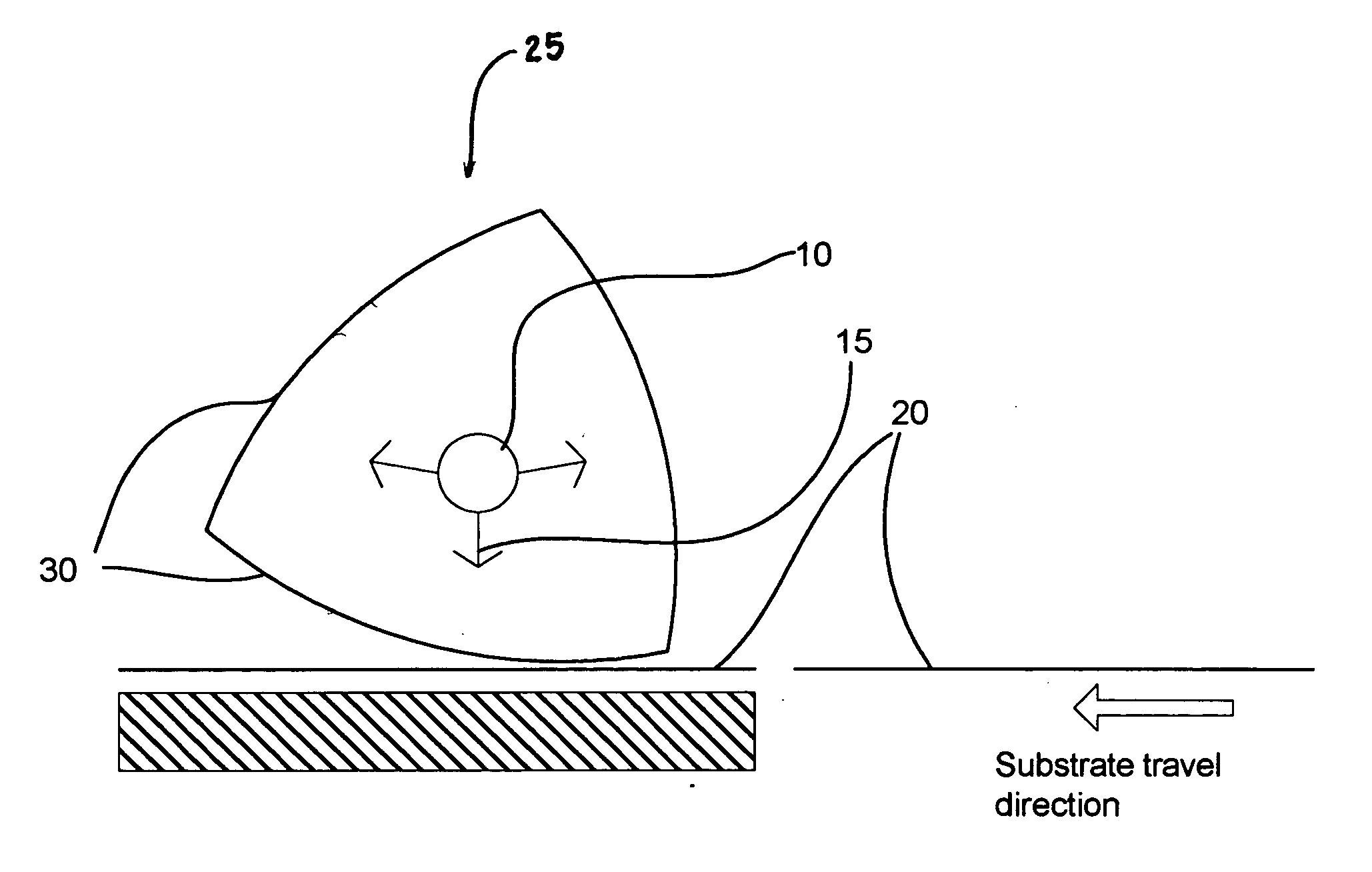
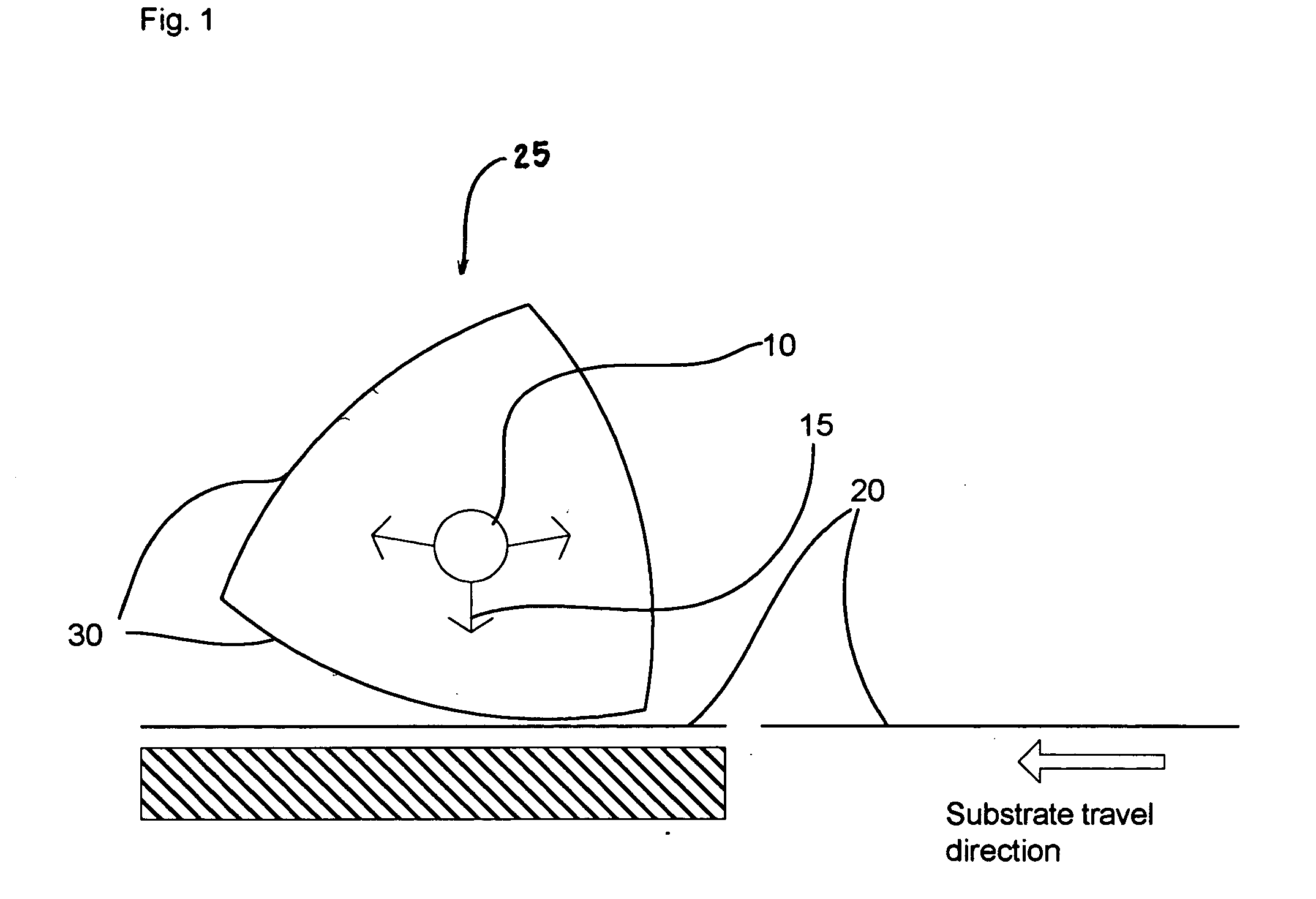
[0022]FIG. 1 depicts substrates 20 being introduced into the patterning device. The curved member 25 includes a patterning stamp 30 on its surfaces, which contains a desired pattern. The curved member 25 is rolled over the substrates 20. Each patterning stamp 30 on the surfaces of the curved member 25 are configured to be the correct size to print the desired pattern onto a single substrate 20. As the patterning stamp 30 rolls over a substrate 20, the illumination means 10 illuminates the substrate via the patterned surface 30.

[0023] Exposure radiation 15 is the illumination radiating in the correct direction in order to set the resist via the stamp pattern. The resist on the substrate 20 sets where the pattern allows the exposure radiation 15 to be transmitted through the curved member 25 wall. The system, in some ways, is analogous to a newspaper printing system except that instead of a round cylinder, a Wankel motor-shaped cylinder is used. In this manner, the surfaces of the cu...


PUM

PropertyMeasurementUnit
wavelengthaaaaaaaaaa

Abstract

The printing apparatus, presented herein, comprises a patterning device having a curved member that supports a stamp on its surface. The curved member is adapted to roll over a substrate to be printed on to transfer the pattern onto the substrate. An illumination system directs light onto the region of the substrate that is being printed in order to set a layer of resist, which has been sprayed onto the substrate. The light is directed via a pattern that is made on the surface of the stamp, thereby transferring the pattern to the substrate.

Description

BACKGROUND OF THE INVENTION [0001] 1. Field of the Invention [0002] The present invention relates to a printing apparatus and a device manufacturing method. [0003] 2. Description of the Related Art [0004] Lithographic apparatus can be used, for example, in the manufacture of integrated circuits (ICs). In such a case, a patterning device may be used to generate a desired circuit pattern corresponding to an individual layer of the IC, and this pattern can be imaged onto a target portion (e.g. comprising one or more dies) on a substrate (silicon wafer) that has been coated with a layer of radiation-sensitive material (resist). [0005] In general, a single substrate will contain a network of adjacent target portions that are successively exposed. Known lithographic apparatus include so-called steppers, in which each target portion is irradiated by exposing an entire pattern onto the target portion in one go, and so-called scanners, in which each target portion is irradiated by scanning t...

Claims


Application Information

Patent Timeline
Patent Type & Authority Applications(United States)
IPC IPC(8): G03F7/20B05C1/06B05C1/08B05D3/00H01L21/027
CPCB82Y10/00G03F7/0002B82Y40/00
Inventor SIMON, KLAUS
Owner ASML NETHERLANDS BV
Why Eureka
Try Eureka