

Plasma display apparatus
- Summary
- Abstract
- Description
- Claims
- Application Information
AI Technical Summary
Benefits of technology
Problems solved by technology
Method used
Image

Examples
first embodiment
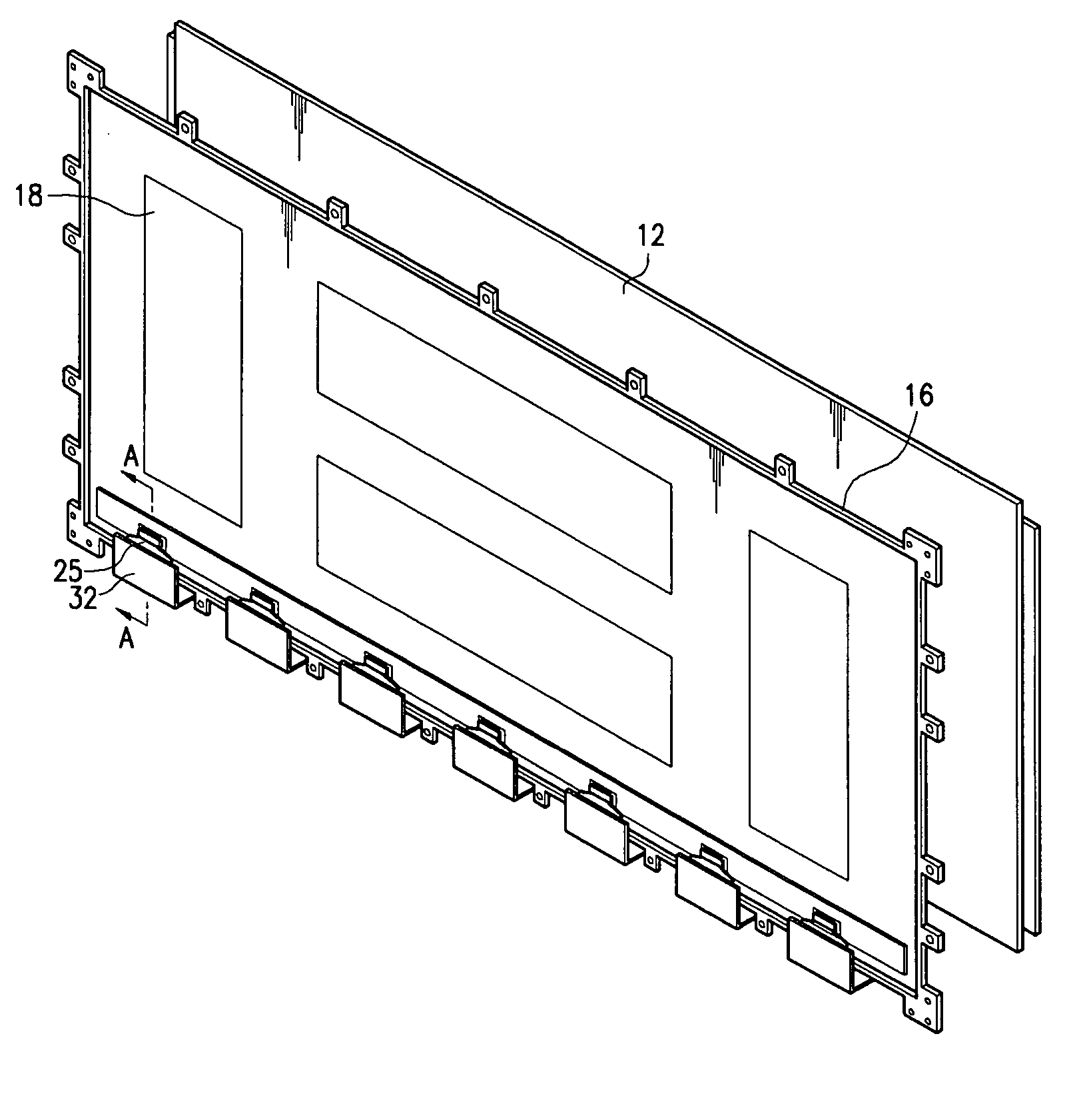
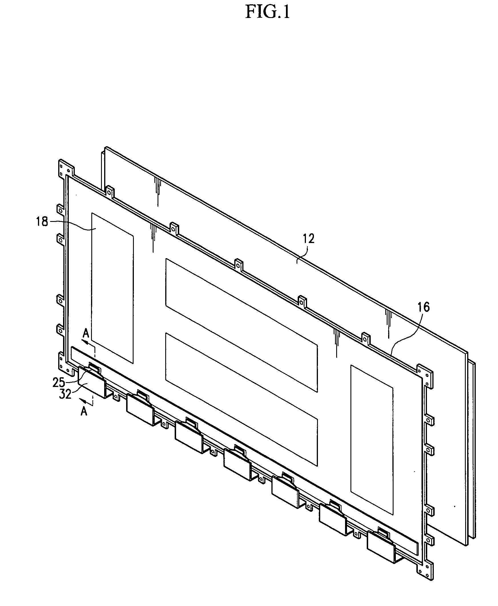
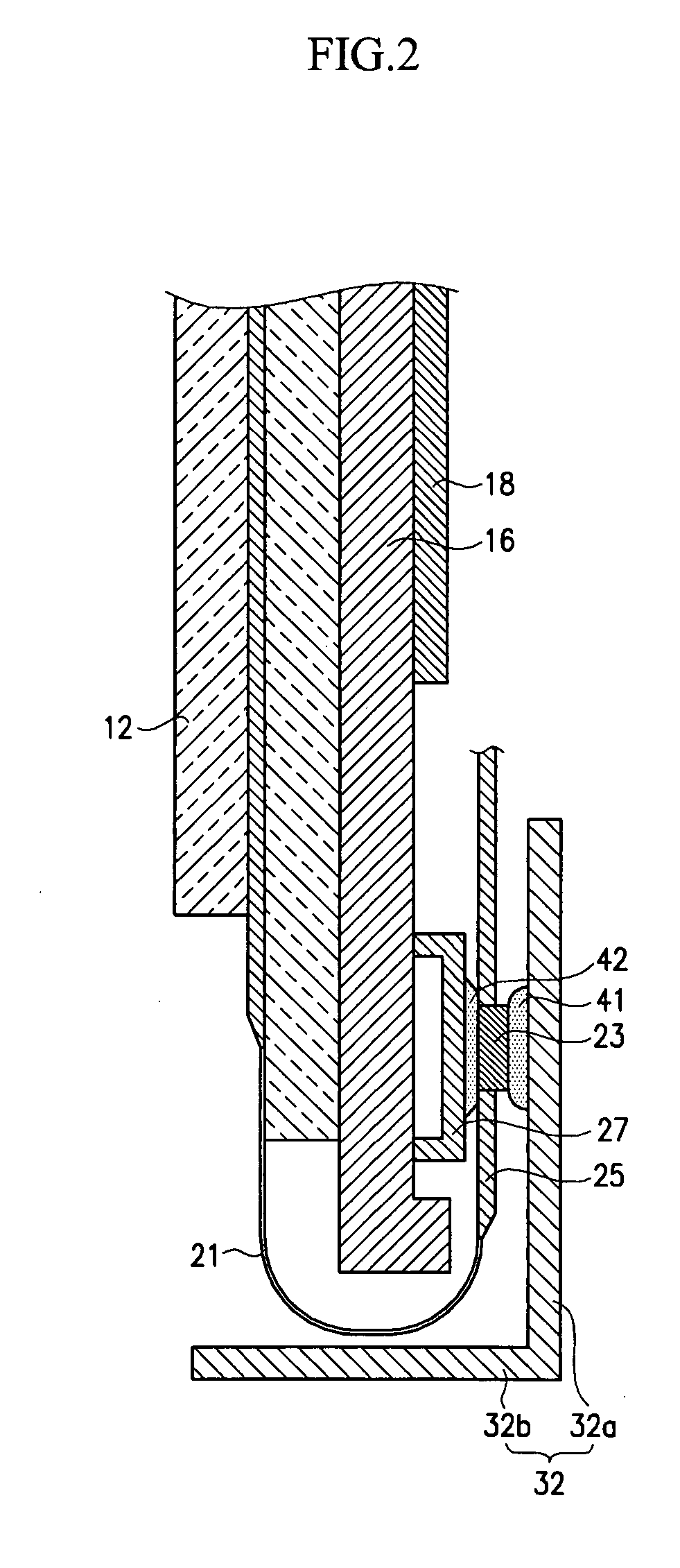
[0039]FIG. 1 is an exploded perspective view of a plasma display apparatus having a heat dissipating structure for a driver IC according to the present invention, and FIG. 2 is a cross-sectional view taken along the A-A line of FIG. 1.
[0040] With reference to FIG. 1 and FIG. 2, the plasma display apparatus includes a plasma display panel 12 (referred to hereinafter simply as a “PDP”), and a chassis base 16. The chassis base 16 is made of Cu, Fe, or the like, and the PDP 12 is mounted on one side surface thereof and a driving circuit 18 is mounted on the other side surface of the chassis base 16.
[0041] The PDP 12 of the plasma display device is mounted on a chassis base (not shown), with a front cover (not shown) on the outside of the PDP 12 and a rear cover (not shown) on the outside of a chassis base.
[0042] Electrodes extending from the periphery of the PDP 12 are electrically connected to the driving circuit 18 to receive the signals required for driving the PDP 12.
[0043] A dri...
second embodiment
[0054]FIG. 3 is a cross-sectional view of a heat dissipating structure for a driver IC 23 according to the present invention.
[0055] With reference to FIG. 3, a plasma display apparatus according to the second embodiment of the present invention has a structure in which a third thermal conduction medium 43 in the form of a sheet is interposed between the driver IC 23 and the first thermal conduction medium 41.
[0056] In this embodiment, the third thermal conduction medium 43 is disposed between the driver IC 23 and a first portion 32a of a cover plate 32, and the first thermal conduction medium 41 is disposed between the first portion 32a of the cover plate 32 and the thermal conduction medium 41. The cover plate 32 can also have a second portion 32b extending from one distal end of the first portion 32a toward the peripheral edge of the PDP 12 and intersecting with the first portion 32a so as to support the second portion 32b.
[0057] The third thermal conduction medium 43 can be for...
third embodiment
[0061]FIG. 4 is an exploded perspective view of a plasma display apparatus according to the present invention, and FIG. 5 is a partial sectional perspective view of the chassis base shown in FIG. 4. FIG. 6 is a combinatorial sectional view of the plasma display apparatus shown in FIG. 4.
[0062] As shown in FIGS. 4 to 6, the plasma display apparatus 100 basically includes a PDP 12, and a chassis base 16. A front cover (not shown) externally surrounds the PDP 12, and a rear cover (not shown) externally surrounds the chassis base 16. The front and the rear covers are combined with each other to thereby complete a plasma display apparatus set.
[0063] The chassis base 16 is formed with aluminum, copper, or iron. The PDP 12 is mounted on a one-sided surface of the chassis base 16, and a driving circuit unit 18 is mounted on the opposite-sided surface of the chassis base 16 to drive the PDP 12.
[0064] The PDP 12 displays the desired images by exciting phosphors with the vacuum ultraviolet r...
PUM
 Abstract
Description
Claims
Application Information