Method and system for precisely positioning a waist of a material-processing laser beam to process microstructures within a laser-processing site

a laser beam and microstructure technology, applied in the direction of photomechanical equipment, manufacturing tools, instruments, etc., can solve the problems of insufficient link cutting, small device affecting the geometry of links, and possible substrate damage, so as to improve focus control, reduce the effect of spot size and small geometry

Inactive Publication Date: 2005-09-15
ELECTRO SCI IND INC
View PDF58 Cites 38 Cited by
  • Summary
  • Abstract
  • Description
  • Claims
  • Application Information

AI Technical Summary

Benefits of technology

[0028] The step of providing may include the steps of reducing power of the material-processing laser beam to obtain a probe laser beam and utilizing the probe laser beam to perform the step of measuring.
[0029] Further in carrying out the above objects and other objects of the present invention, a system for precisely positioning a waist of a material-processing laser beam to dynamically compensate for local variations in height of microstructures located on a plurality of objects spaced apart within a laser-processing site is provided. The system includes a focusing lens subsystem for focusing a laser beam along an optical axis, a first actuator for moving the objects in a plane, and a second actuator for moving the focusing lens subsystem along the optical axis. The system further includes a first controller for controlling the first actuator based on reference data which represents 3-D locations of microstructures to be processed within the site, and a second controller for controlling of the second actuator also based on the reference data. The first and second actuators controllably move the objects and the focusing lens subsystem, respectively, to precisely position the waist of the laser beam and the objects so that the waist substantially coincides with the 3-D locations of the microstructures within the site.
[0044] The height information will preferably be obtained from the same laser and optical path used for processing, but with reduced power (with a modulator used to reduce the power and avoid damage to the surface).
[0070] A system of the present invention is able to operate with smaller spot sizes (which require better focus control) and thereby process devices with smaller geometry than prior memory repair systems due in part to superior focus control.
[0071] Dynamic Focus allows a system of the present invention to adapt to the non-parallel and non-planar topology that is typically found on real wafers and maintain acceptable focus over the full extent of a die site.

Problems solved by technology

This manufacture of smaller devices affects the geometry of the links allocated for laser redundancy.
A defocused spot reduces the energy that is delivered to the target link possibly leading to insufficient cutting of the link.
A defocused spot may also place more laser energy on adjacent links or on the intervening substrate leading to possible substrate damage.
At some level of defocus, the laser cutting process is no longer viable.
This presents a problem in that the wafers seldom are flat (planar) and parallel to the focal plane.
The process or sensor used to measure focus may exhibit errors.
The mechanism used to provide relative motion between the wafer surface and focal plane may exhibit errors.
The problem encountered at the time was due to the packaged die being significantly non-parallel to the surrounding package (typically pressure sensors).
One problem of this approach is that the auto-collimator worked best when it could be directed at a large “planar” object.
It would not be possible to find such a region on a typical IC found in memory repair applications.
In 1994, GSI developed a different approach to handle thin-film trimming on “tilted die.” The problem was again due to trimming on packaged IC (pressure sensors).
In this case, the specifics of the customer's device precluded the use of a tilting Z-stage.
Also, the absence of suitable target structures for the auto-collimator on certain customer's devices forced GSI to develop the multi-site focus algorithm.

Method used


Image

  • Method and system for precisely positioning a waist of a material-processing laser beam to process microstructures within a laser-processing site
  • Method and system for precisely positioning a waist of a material-processing laser beam to process microstructures within a laser-processing site
  • Method and system for precisely positioning a waist of a material-processing laser beam to process microstructures within a laser-processing site

Examples


Embodiment Construction

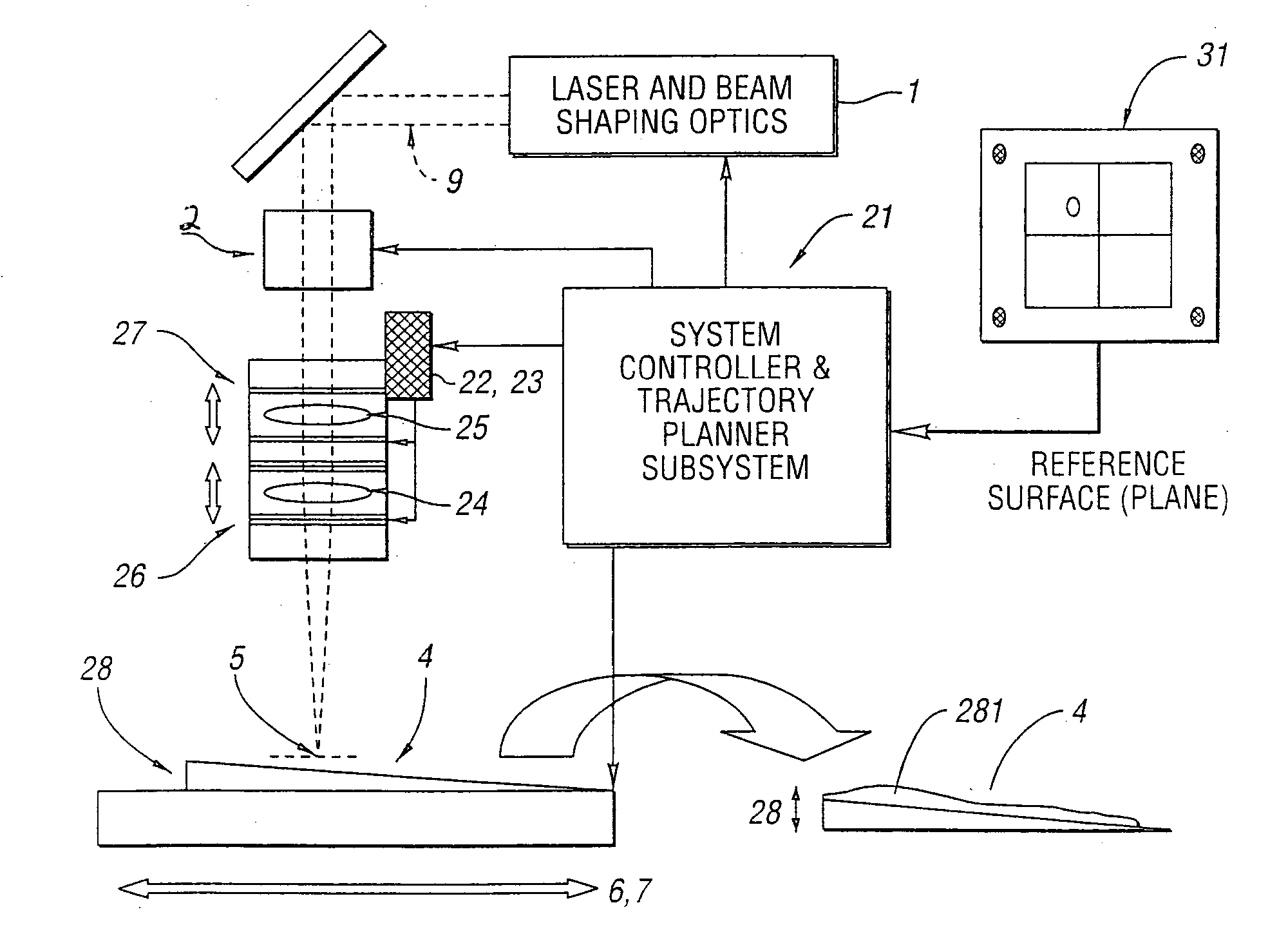
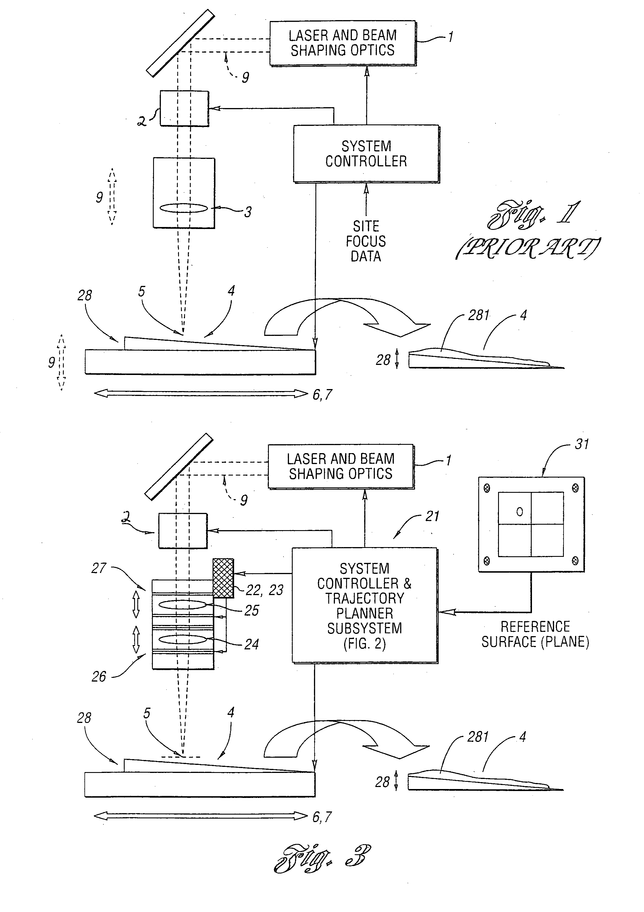
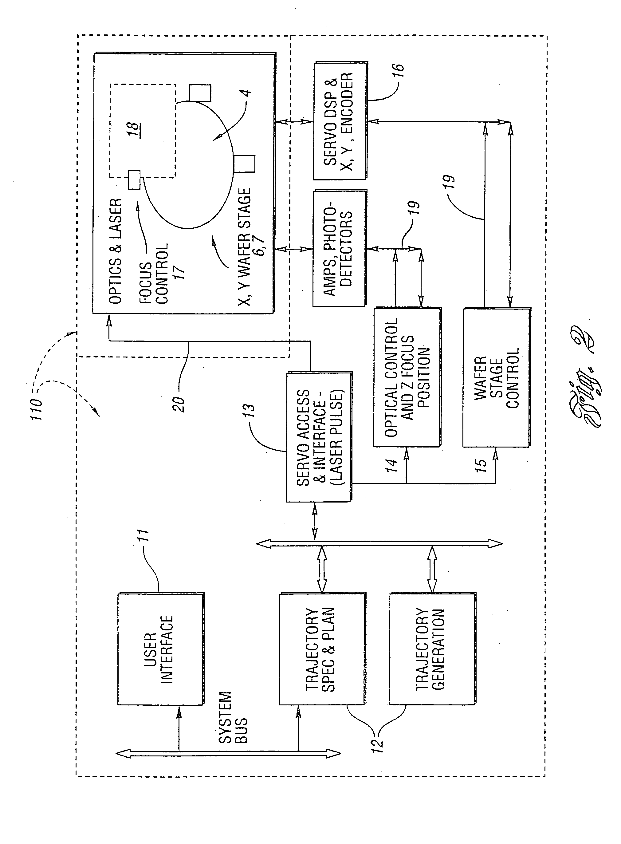
[0085] A preferred system of the present invention is shown in FIG. 2. A wafer 4 is positioned within the laser processing system 110 and database information from the user interface 11 is provided to identify the links (33 in FIG. 4) on the wafer which are to be ablated to repair defective memory cells.

[0086] Referring to FIG. 3, wafers exhibit wedge 28 (i.e. a plane that is tilted with respect to the focal plane) and non-planar topology 281 which requires compensation. The wedge 28 and local curvature 281 are exaggerated in scale for the purpose of illustration. Based upon the specified locations of the defective cells regions are identified on the wafer (33 in FIG. 4) in reference height data is to be obtained. Such locations may be “bare wafer” regions that have little surface texture or other suitably defined regions that are generally selected to match the imaging and processing capabilities of the measurement sensor. Typically depth information will be obtained using a “dept...


PUM

PropertyMeasurementUnit
diameteraaaaaaaaaa
velocityaaaaaaaaaa
beam waist diameteraaaaaaaaaa

Abstract

A high-speed method and system for precisely positioning a waist of a material-processing laser beam to dynamically compensate for local variations in height of microstructures located on a plurality of objects spaced apart within a laser-processing site are provided. In the preferred embodiment, the microstructures are a plurality of conductive lines formed on a plurality of memory dice of a semiconductor wafer. The system includes a focusing lens subsystem for focusing a laser beam along an optical axis substantially orthogonal to a plane, an x-y stage for moving the wafer in the plane, and a first air bearing sled for moving the focusing lens subsystem along the optical axis.

Description

CROSS REFERENCE TO RELATED APPLICATIONS [0001] This application is related to provisional patent application entitled “Trajectory Generation And Link Optimization”, filed the same day as the present application. Also, this application is related to U.S. patent applications entitled “Precision Positioning Apparatus” filed on Sep. 18, 1998 and having U.S. Ser. No. 09 / 156,895, and “Energy Efficient Laser-Based Method and System for Processing Target Material” filed on Dec. 28, 1999 and having U.S. Ser. No. 09 / 473,926.TECHNICAL FIELD [0002] This invention generally relates to methods and systems for high speed laser processing (machining, cutting, ablating) microstructures. More specifically, this invention relates to methods and systems for precisely positioning a waist of a material-processing laser beam to process microstructures within a laser-processing site. Semiconductor memory repair is a specific application where precise positioning in depth of the beam waist of the laser beam...

Claims


Application Information

Patent Timeline
Patent Type & Authority Applications(United States)
IPC IPC(8): B23K26/04B23K26/08B23K101/40G03F7/20H01L21/82
CPCB23K26/04B23K26/046B23K26/0853B23K26/02G03F7/70041G03F7/70725B23K26/043B23K2201/40B23K2101/40H01L21/30
Inventor HUNTER, BRADLEY L.CAHILL, STEVEN P.EHRMANN, JONATHAN S.PLOTKIN, MICHAEL
Owner ELECTRO SCI IND INC
Why Eureka
Try Eureka