Light-emitting diode with micro-lens layer

Inactive Publication Date: 2005-09-15
OPTO TECH
View PDF8 Cites 22 Cited by
  • Summary
  • Abstract
  • Description
  • Claims
  • Application Information

AI Technical Summary

Benefits of technology

[0005] Thus, it is a keynote of the present invention to devise a novel light-emitting diode capable of improvin

Problems solved by technology

This would further result in a low light-drawing efficiency and a degradation of the luminance for the light

Method used


Image

  • Light-emitting diode with micro-lens layer
  • Light-emitting diode with micro-lens layer
  • Light-emitting diode with micro-lens layer

Examples


Embodiment Construction

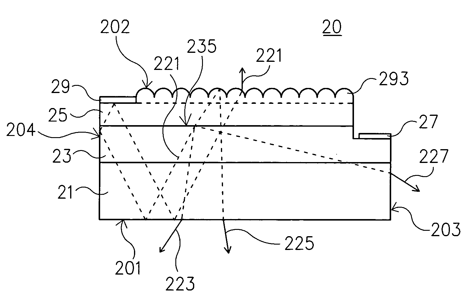
[0017] Referring to FIG. 2, a light-emitting diode according to a preferred embodiment of the present invention is depicted. As shown, the light-emitting diode 20 with a micro-lens layer according to the present invention includes: a die substrate 21, a second epitaxy layer 23 deposited on the top surface of the die substrate 21, at least one first epitaxy layer 25 deposited on a portion of the top surface of the second epitaxy layer 23 with a light-emitting active region formed between the first epitaxy layer 25 and the second epitaxy layer 23, a second electrode 27 formed on a portion of the top surface of the second epitaxy layer 23, at least one first electrode 29 formed on a portion of the top surface of the first epitaxy layer 25, and a micro-lens layer 293 consisted of a plurality of micro-lens and formed on a portion the top surface of the first epitaxy layer 25.

[0018] In the present embodiment, the micro-lens layer 293 has a curvature which is constituted by a plurality of...


PUM


Abstract

A light-emitting diode with a micro-lens layer, includes a die substrate, a second epitaxy layer deposited on the top surface of the die substrate, a first epitaxy layer deposited on a portion of the top surface of the second epitaxy layer, a second electrode formed on a portion of the top surface of the second epitaxy layer, a first electrode formed on a portion of the top surface of the first epitaxy layer, and a micro-lens layer mounted on a portion of the top surface of the first epitaxy layer. The micro-lens layer can change the projection angle and the projection path of the light beams radiated within the light-emitting diode in virtue of the diffusion effect caused by the micro-lens, and thereby improving the light-drawing efficiency and the luminance of the light-emitting diode.

Description

FIELD OF THE INVENTION [0001] The present invention is related to a light-emitting diode, and more particularly to a light-emitting diode with a micro-lens layer for allowing the light beams radiated within the light-emitting diode to change their projection angle and projection path by the diffusion effect caused by the micro-lens. BACKGROUND OF THE INVENTION [0002] As is well known in the prior art, a light-emitting diode has been widely employed in computer peripherals, communication products, and other electronic device because of its light weight, low power consumption, and prolonged longevity. [0003] A conventional light-emitting diode is depicted in FIG. 1. As shown in FIG. 1, the light-emitting diode 10 includes a die substrate 11, a second epitaxy layer 13 deposited on the top surface of the die substrate 11, a first epitaxy layer 15 deposited on a portion of the top surface of the second epitaxy layer 13, a second electrode 17 formed on the other portion of the top surface...

Claims


Application Information

Patent Timeline
IPC IPC(8): H01L29/22
CPCH01L33/20
Inventor LIN, MING-DERLIN, SAN BAO
Owner OPTO TECH
Why Eureka
Try Eureka