Transistor of a semiconductor device having a punchthrough protection layer and methods of forming the same

a technology of protection layer and transistor, which is applied in the direction of semiconductor devices, semiconductor/solid-state device details, electrical devices, etc., can solve the problems of unstable interfacial state of transistors, leakage current, and inability to improve the punching between the source region and the drain region of the reduction of design rules

Active Publication Date: 2005-09-15
SAMSUNG ELECTRONICS CO LTD
View PDF2 Cites 14 Cited by
  • Summary
  • Abstract
  • Description
  • Claims
  • Application Information

AI Technical Summary

Benefits of technology

[0012] According to some embodiments of the invention, transistors of a semiconductor device and a DRAM cell have a punchthrough protection layer in a channel-portion hole, suitable for preventing the punchthrough of a source and a drain region of a transistor.

Problems solved by technology

This reduction tends to create problems, such as a punchthrough between the source and the drain region, as explained below.
However, although the transistor having the channel-portion hole can increase an integration degree of a semiconductor device with the increase of the length of the channel region, a punchthrough between the source region and the drain region associated with the reduction of the design rule is not improved.
The transistor may have an unstable interfacial state along the epitaxial layer defining the trench due to the etching process.
The unstable interface of the epitaxial layer becomes a part of a channel region of the transistor, thereby causing a leakage current during the operation of the semiconductor device.
Further, the method discloses a method of forming a transistor using different oxide layers on a bottom and a sidewall of the trench as the gate oxide layer, but the oxide layers inside the trench may increase the leakage current and decrease a breakdown voltage of the gate oxide layer due to the different oxide layers.

Method used


Image

  • Transistor of a semiconductor device having a punchthrough protection layer and methods of forming the same
  • Transistor of a semiconductor device having a punchthrough protection layer and methods of forming the same
  • Transistor of a semiconductor device having a punchthrough protection layer and methods of forming the same

Examples


Embodiment Construction

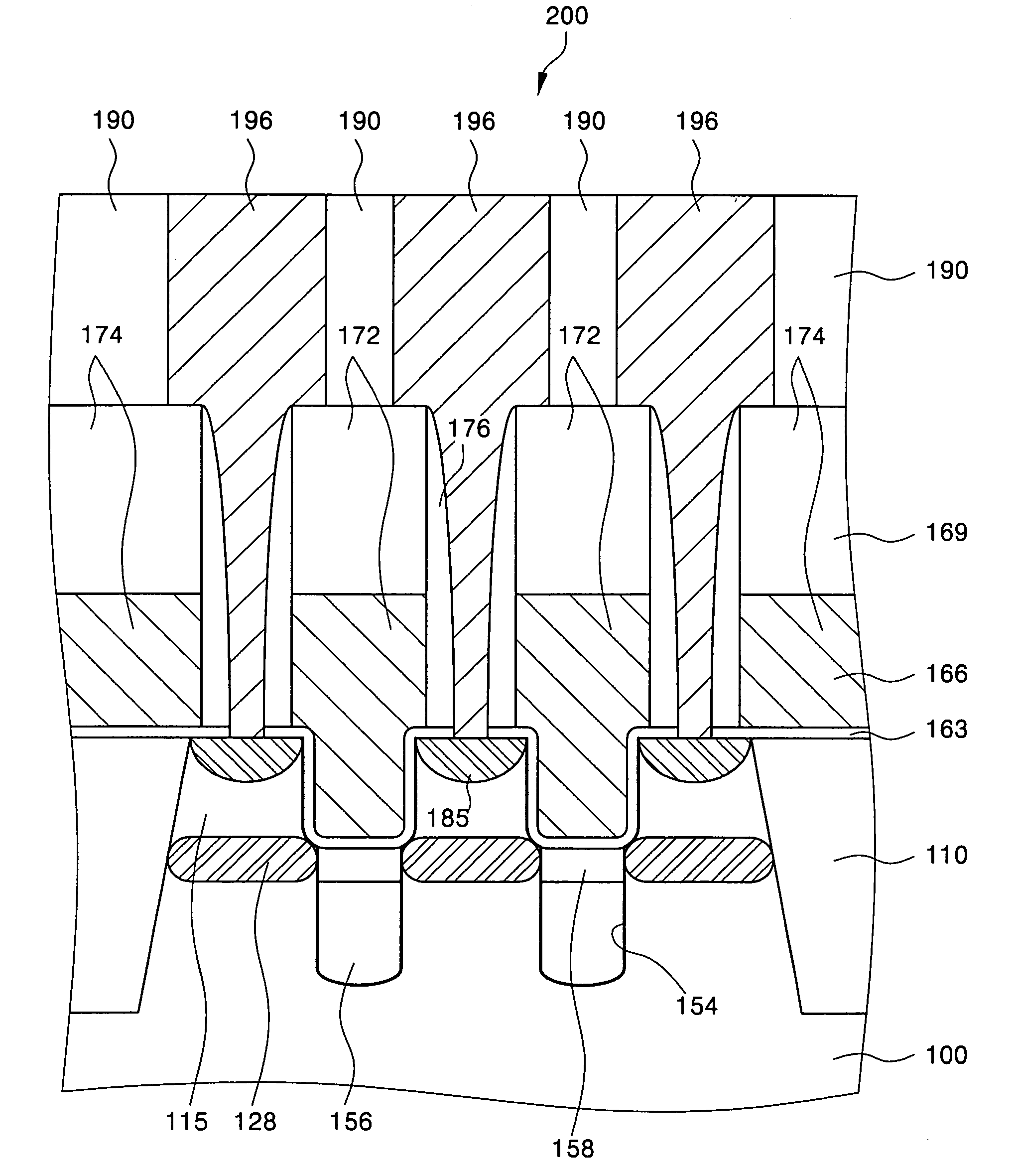
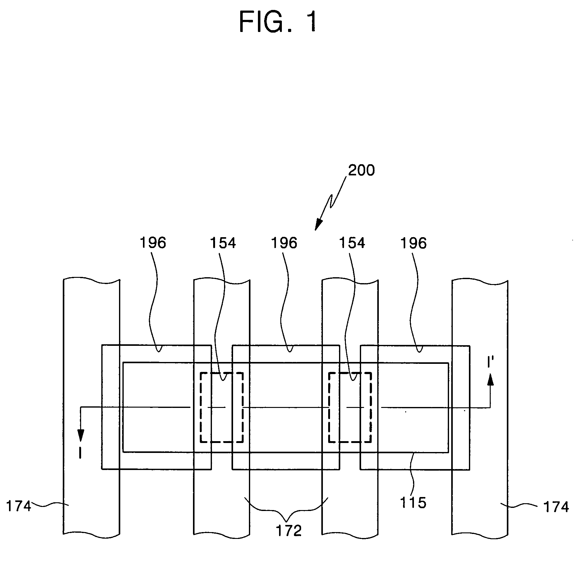
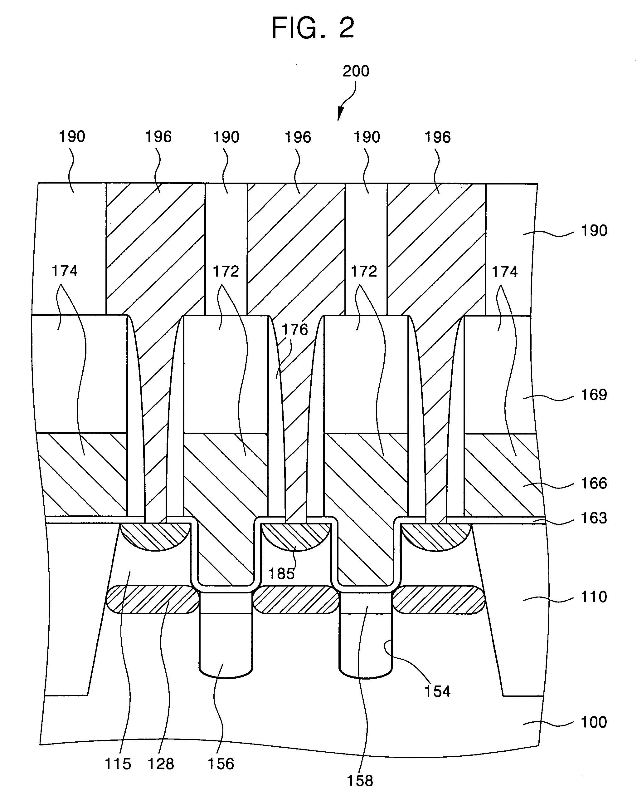
[0018]FIG. 1 is a layout of a transistor of a DRAM cell according to exemplary embodiments of the invention, and FIG. 2 is a sectional view of a transistor of a DRAM cell taken along line I-I′ of FIG. 1.

[0019] Referring to FIGS. 1 and 2, a device isolation layer 110 is disposed in a semiconductor substrate 100 having a DRAM cell array region 200. The device isolation layer 110 isolates an active region 115. The semiconductor substrate 100 preferably has a P conductivity type, but the semiconductor substrate 100 may instead have an N conductivity type.

[0020] At least two channel-portion holes 154 are disposed extending downward from a main surface of the semiconductor substrate 100 of the active region 115, and each of the channel-portion holes 154 has a trench shape. Upper portions of the channel-portion holes 154 are preferably greater in width than lower portions thereof. Alternatively, the upper portions of the channel-portion holes 154 may be smaller in width than the lower po...


PUM


Abstract

According to some embodiments of the invention, transistors of a semiconductor device have a punchthrough protection layer, and methods of forming the same are provided. A channel-portion hole extends downward from a main surface of a semiconductor substrate. A punchthrough protection layer and a channel-portion layer are sequentially formed at a lower portion of the channel-portion hole. A word line pattern fills an upper portion of the channel-portion hole, and is formed on the semiconductor substrate. The word line pattern is formed to have a word line and a word line capping layer pattern stacked thereon, and the channel-portion layer is a channel region. The punchthrough protection layer can reduce a leakage current of a capacitor of the transistor embodied in a DRAM.

Description

CROSS-REFERENCE TO RELATED APPLICATION [0001] This patent application claims priority from Korean Patent Application No. 10-2004-0016272, filed Mar. 10, 2004, the contents of which are hereby incorporated by reference in their entirety. BACKGROUND OF INVENTION [0002] 1. Technical Field [0003] The invention relates to transistors of a semiconductor device and methods of forming the same, and more particularly, to transistors of a semiconductor device having a punchthrough protection layer and methods of forming the same. [0004] 2. Discussion of the Related Art [0005] Generally, a transistor includes a word line pattern, source / drain regions and a channel region. The channel region is disposed in the semiconductor substrate under the word line pattern, and the source / drain regions are disposed in the semiconductor substrate so that they overlap the word line pattern. The word line pattern is also disposed on the semiconductor substrate along with the source / drain regions and the chann...

Claims


Application Information

Patent Timeline
Patent Type & Authority Applications(United States)
IPC IPC(8): H01L29/78H01L21/336H01L21/8242H01L27/108
CPCH01L27/0207H01L29/1083H01L27/10876H01L27/10861H10B12/038H10B12/053H01L29/0847H10B12/488H01L29/78696H01L21/02293
Inventor SEO, HYEOUNG-WONKIM, KI-NAMYANG, WOUN-SUCKSONG, DU-HEON
Owner SAMSUNG ELECTRONICS CO LTD
Why Eureka
Try Eureka