Methods of fabricating a semiconductor device having a metal gate pattern

a metal gate and metal gate technology, applied in semiconductor devices, semiconductor/solid-state device details, electrical devices, etc., can solve the problems of damage to the exposed surface of silicon layer and the edges of metal gate layer, and achieve the effect of suppressing diffusion of oxidants

US20060270205A1Inactive Publication Date: 2006-11-30SAMSUNG ELECTRONICS CO LTD
3 Cites 5 Cited by

Patent Information

Authority / Receiving Office
US · United States
Patent Type
Applications(United States)
Current Assignee / Owner
Publication Date
2006-11-30
Estimated Expiration
Not applicable · inactive patent

Smart Images

  • Figure 1
    Figure 1
  • Figure 2
    Figure 2
  • Figure 3
    Figure 3
Patent Text Reader

Abstract

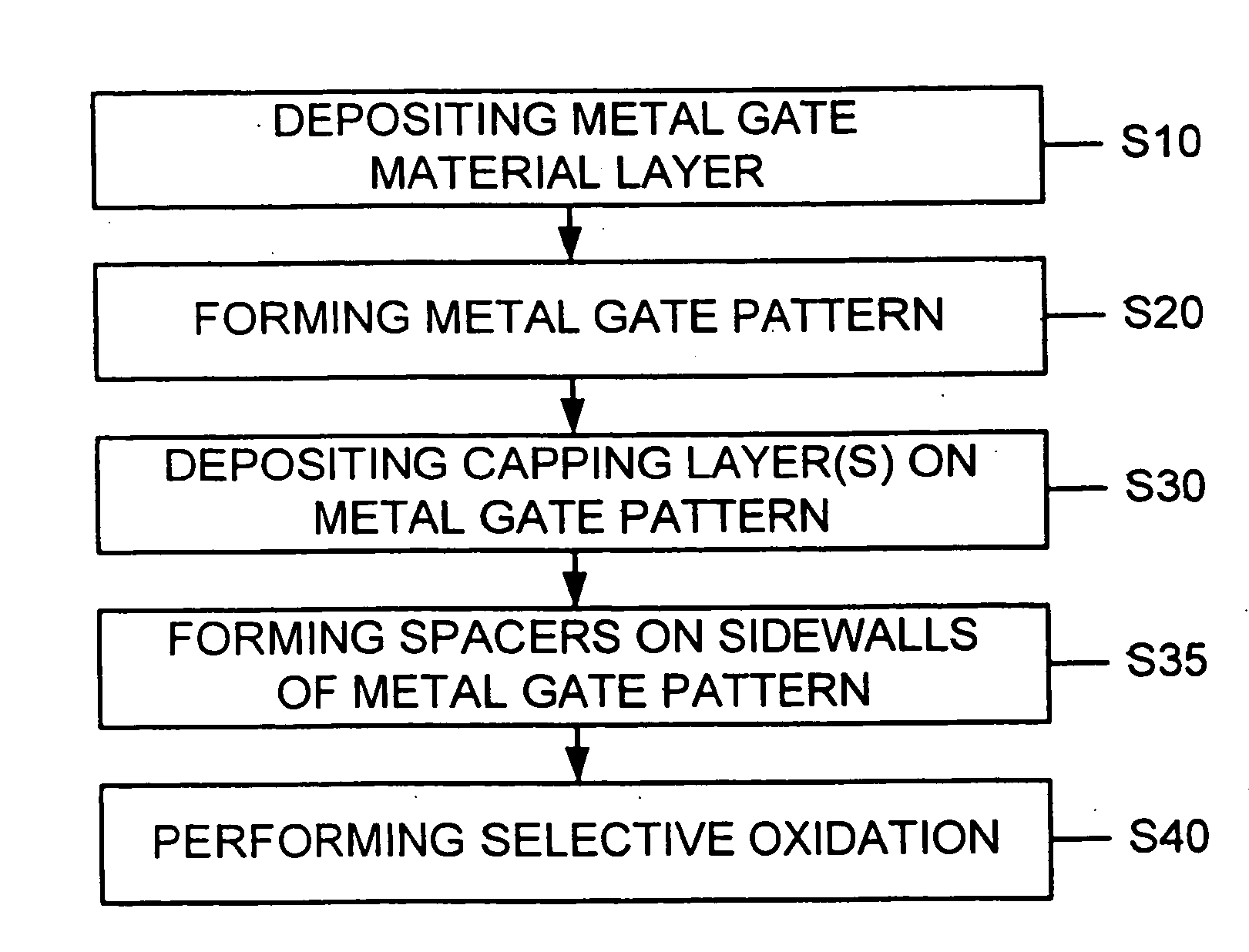
A method of fabricating a semiconductor device having a metal gate pattern is provided in which capping layers are used to control the relative oxidation rates of portions of the metal gate pattern during a oxidation process. The capping layer may be a multilayer structure and may be etched to form insulating spacers on the sidewalls of the metal gate pattern. The capping layer(s) allow the use of a selective oxidation process, which may be a wet oxidation process utilizing partial pressures of both H2O and H2 in an H2-rich atmosphere, to oxidize portions of the substrate and metal gate pattern while suppressing the oxidation of metal layers that may be included in the metal gate pattern. This allows etch damage to the silicon substrate and edges of the metal gate pattern to be reduced while substantially maintaining the original thickness of the gate insulating layer and the conductivity of the metal layer(s).
Need to check novelty before this filing date? Find Prior Art

Description

CROSS REFERENCE TO RELATED APPLICATIONS

[0001] This U.S. non-provisional application claims priority under 35 U.S.C. § 119 to Korean Patent Application No. 2002-57456, filed on Sep. 19, 2002, in the Korean Intellectual Property Office, the contents of which are incorporated herein by reference in their entirety. BACKGROUND OF THE INVENTION

[0002] 1. Field of the Invention

[0003] The present invention relates generally to methods of fabricating semiconductor devices having metal gate patterns, and more particularly to a method of fabricating a semiconductor that includes selective oxidation to reduce damage to the metal gate pattern caused by dry etching.

[0004] 2. Description of the Related Art

[0005] Due to a continuing interest in increasing the integration density of semiconductor devices, the dimensions of various structural elements such as capacitors and gate electrodes utilized to form such semiconductor devices also tend to be reduced. Because of the increase in the integrat...

Examples

Embodiment Construction

[0042] Exemplary embodiments of the present invention will now be described more fully with reference to the accompanying drawings, in which exemplary embodiments of the invention are shown. This invention may, however, be embodied in many different forms and should not be construed as being limited to the exemplary embodiments set forth herein. Rather, these exemplary embodiments are provided so that this disclosure is thorough and complete and fully conveys the concept of the invention to those skilled in the art. In the drawings, the shape of the elements may be exaggerated for clarity, and the same reference numerals in different drawings represent the same elements.

[0043] Further, it will be understood that when a layer is referred to as being “on” another layer or substrate, it can be located directly on the other layer or substrate, or intervening layers may also be present. It will also be understood that when a layer is referred to as being “directly on” another layer or s...