Non-volatile memory, manufacturing method and operating method thereof

a manufacturing method and non-volatile memory technology, applied in the field of semiconductor devices, can solve the problems of adverse impact on the electrical performance of the memory, uneven distribution of electrons injected in the silicon nitride layer, and data misjudgment, so as to reduce the operation voltage of the memory, inject and pull electrons more quickly, and improve the efficiency

Active Publication Date: 2006-12-28
POWERCHIP SEMICON MFG CORP
View PDF5 Cites 7 Cited by
  • Summary
  • Abstract
  • Description
  • Claims
  • Application Information

AI Technical Summary

Benefits of technology

[0035] In the operating method of the non-volatile memory, the adopted operation mode for programming and erasing has a higher efficiency and is capable of injecting and pu

Problems solved by technology

When erasing data in the EEPROM however, it is likely to over-erase, which leads to misjudgment of data.
Therefore, when programming the memory cell, an abnormal punch-through phenomenon occurs between a drain region and a source region, which has an adverse impact on the electrical performance of the memory.
Since the silicon nitride is able to capture electrons, the electrons injected in the silicon nitride layer would not be evenly distribute

Method used


Image

  • Non-volatile memory, manufacturing method and operating method thereof
  • Non-volatile memory, manufacturing method and operating method thereof
  • Non-volatile memory, manufacturing method and operating method thereof

Examples


Embodiment Construction

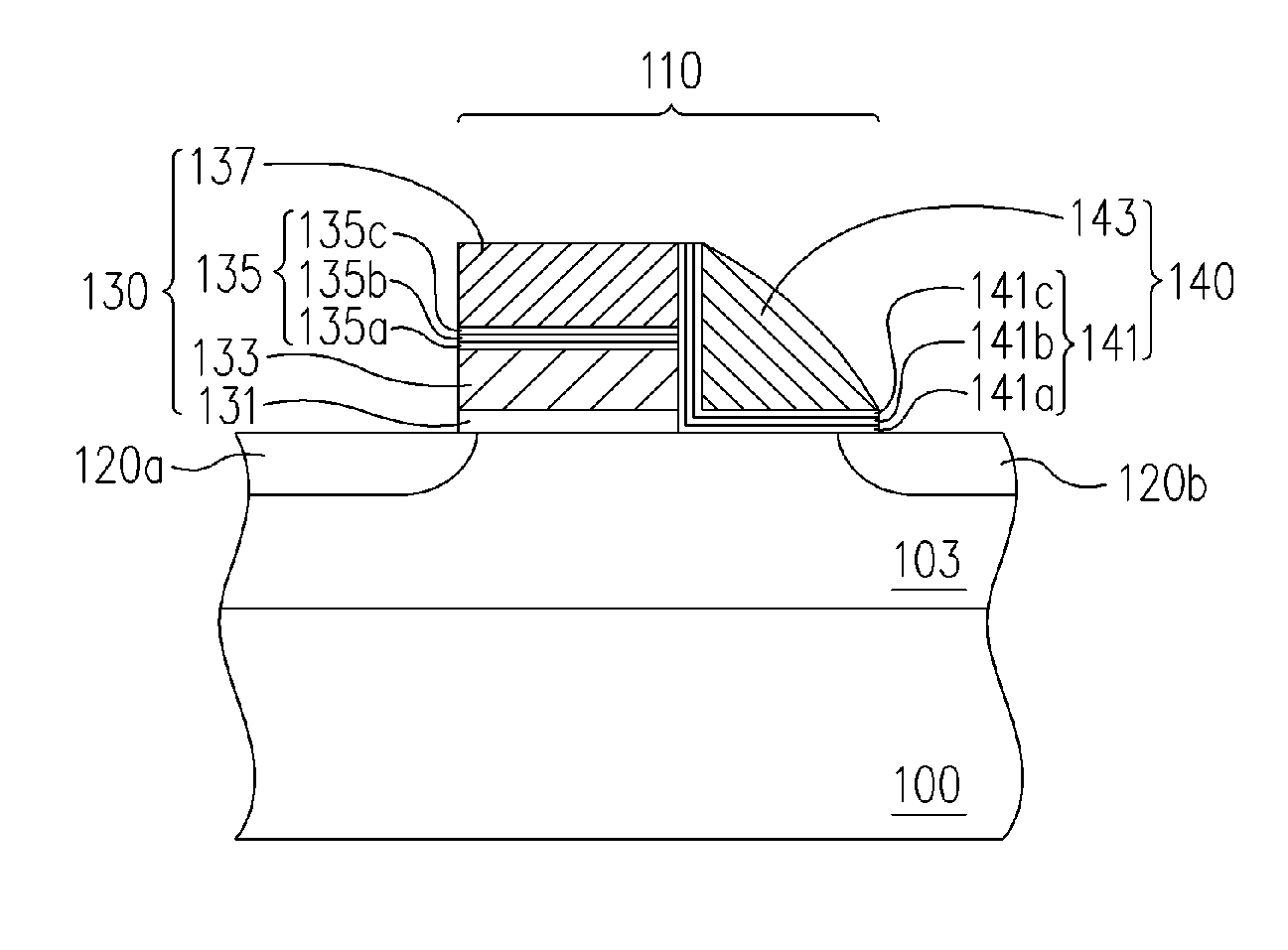
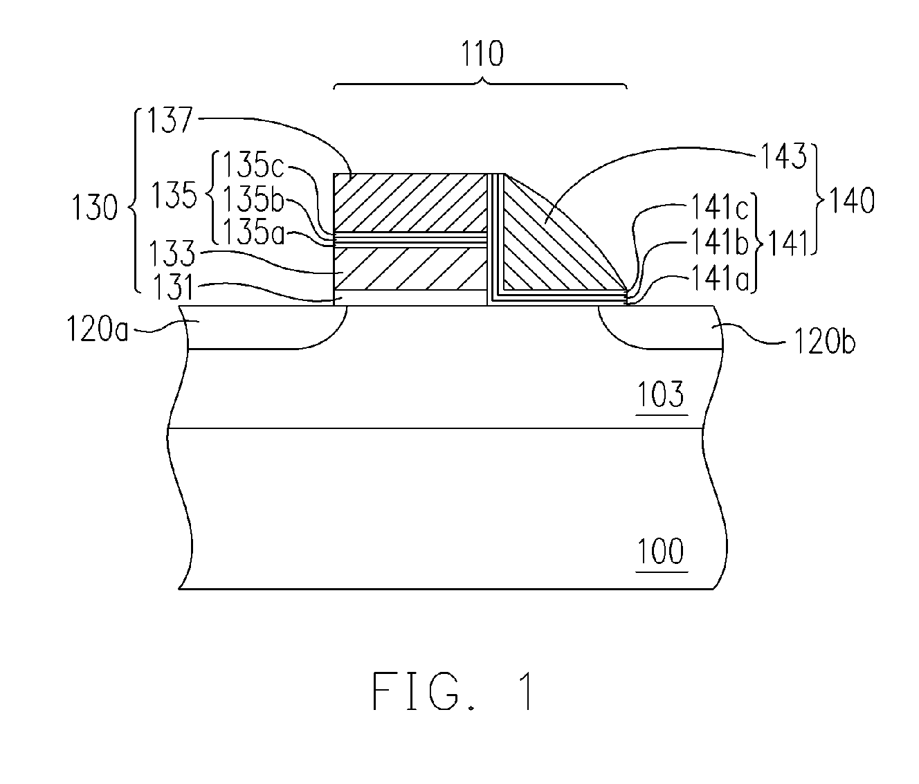
[0044]FIG. 1 is a schematic structural cross-sectional view of a non-volatile memory in an embodiment of the present invention.

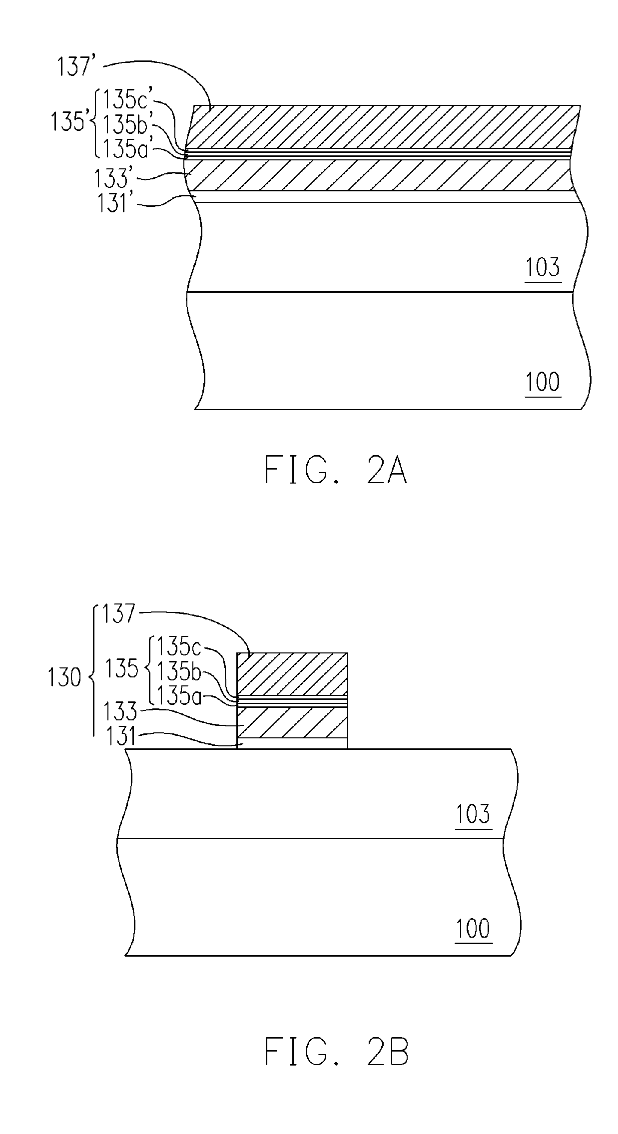
[0045] Referring to FIG. 1, the non-volatile memory includes at least a substrate 100, memory cells 110 and source / drain regions 120a and 120b. The memory cell 110 is disposed on the substrate 100 and includes at least a memory unit 130 and another memory unit 140. Wherein, the memory unit 130, from the substrate 100 up, includes at least a tunneling dielectric layer 131, a floating gate 133, an inter-gate dielectric layer 135 and a control gate 137. The memory unit 140 is disposed on a sidewall of the memory unit 130. The memory unit 140 includes, for example, a control gate 143 and a charge trapping structure 141. The control gate 143 is disposed on a sidewall of the memory unit 130 and the charge trapping structure 141 is disposed between the control gate 143 and the memory unit 130, and between the control gate 143 and the substrate 100. The source / drai...


PUM


Abstract

A non-volatile memory including at least a substrate, a memory cell and source/drain regions is provided. The memory cell is disposed on the substrate and includes at least a first memory unit and a second memory unit. Wherein, the first memory unit, from the substrate up, includes a floating gate and a first control gate. The second memory unit is disposed on a sidewall of the first memory unit and includes a charge trapping layer and a second control gate. The two source/drain regions are disposed in the substrate at both sides of the memory cell.

Description

CROSS-REFERENCE TO RELATED APPLICATION [0001] This application claims the priority benefit of Taiwan application serial no. 94121378, filed on Jun. 27, 2005. All disclosure of the Taiwan application is incorporated herein by reference. BACKGROUND OF THE INVENTION [0002] 1. Field of Invention [0003] The present invention relates to a semiconductor device, and particularly to a non-volatile memory (NVM), a manufacturing method and an operating method thereof. [0004] 2. Description of the Related Art [0005] Among various types of non-volatile memory products, electrically erasable programmable read only memory (EEPROM) is a memory device that has been widely used in personal computers and electronic equipment. Data can be stored, read out or erased from the EEPROM many times and stored data are retained even after power supplying the devices is cut off. [0006] The floating gate and the control gate in a typical EEPROM are made of doped polysilicon. By applying bias voltages to the cont...

Claims


Application Information

Patent Timeline
IPC IPC(8): H01L29/788H01L21/8238
CPCH01L21/28273H01L21/28282H01L27/115H01L29/4232H01L29/42324H01L29/7923H01L29/42344H01L29/66825H01L29/66833H01L29/7887H01L29/42328H01L29/40114H01L29/40117H10B69/00
Inventor WONG, WEI-ZHEYANG, CHING-SUNG
Owner POWERCHIP SEMICON MFG CORP
Why Eureka
Try Eureka