High frequency differential power amplifier

a power amplifier and high frequency technology, applied in the field of high frequency communications, can solve the problems of excessive voltage drop, unsatisfactory output signal degradation, and increase the power consumption of differential amplifiers b>100, and achieve the effect of not consuming excessive power

Active Publication Date: 2005-09-22
SONRAI MEMORY LTD
View PDF54 Cites 18 Cited by
  • Summary
  • Abstract
  • Description
  • Claims
  • Application Information

AI Technical Summary

Benefits of technology

[0015] According to an embodiment of the invention, a high-frequency differential amplifier includes two CMOS inverters and biasing circuitry. The CMOS inverters apply a desired gain to a differential input signal based on the transconductance and output impedance values of the transistors making up the inverters. Meanwhile, the biasing circuitry applies linear biasing to the CMOS inverters without consuming excessive power.
[0016] The biasing circuitry provides a DC feedback loop that forces a DC bias voltage to appear at the outputs of the inverters. By selecting the DC bias voltage to be between the logic HIGH and LOW output levels of the inverters, the inverters can be forced to operate in their linear region. AC signals at the inputs of the inverters will then be amplified by the inverters without distortion (clipping), so long as the amplitudes of the AC signals are not large enough to drive either inverter out of its linear mode of operation.
[0018] This DC control provided by each op-amp ensures that the inverters will operate in their linear regions as long as the input signals are not large enough to push the transistors of the inverters into saturation. By setting the reference voltage equal to half of the voltage difference between the upper and lower supply voltages provided to the amplifier, the output range of the amplifier can be maximized.

Problems solved by technology

Unfortunately, because of the common-source implementations used in differential amplifier 100, increasing resistance R_SET and / or increasing transconductance gm can result in undesirable output signal degradation.
Similarly, increasing transconductances gm111 and gm112 (and possibly increasing bias current I_BIAS) will result in larger current magnitudes through resistors R1_SET and R2_SET, respectively, which once again can lead to excessive voltage drops.
Another problematic issue relates to the fact that increasing the size of resistors R1_SET and R2_SET and / or increasing current I_BIAS can significantly increase the power consumption of differential amplifier 100.
This power inefficiency is generally undesirable, and can be particularly problematic in devices that run off of a self-contained power supply (a battery).
For example, using amplifier 100 in a cellular telephone to reduce the overall cost of the phone may result in an unacceptable decrease in talk time for that phone.

Method used


Image

  • High frequency differential power amplifier
  • High frequency differential power amplifier
  • High frequency differential power amplifier

Examples


Embodiment Construction

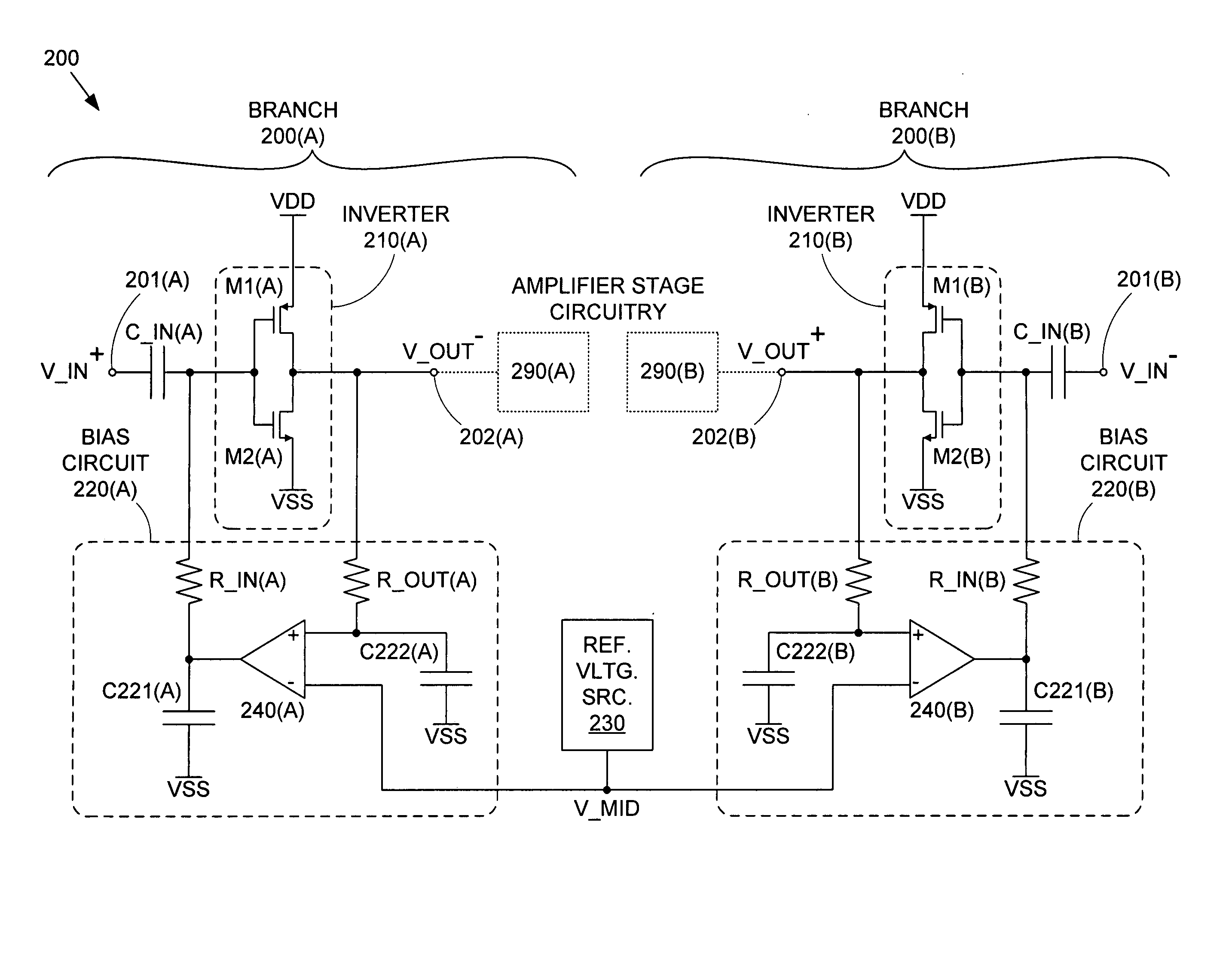
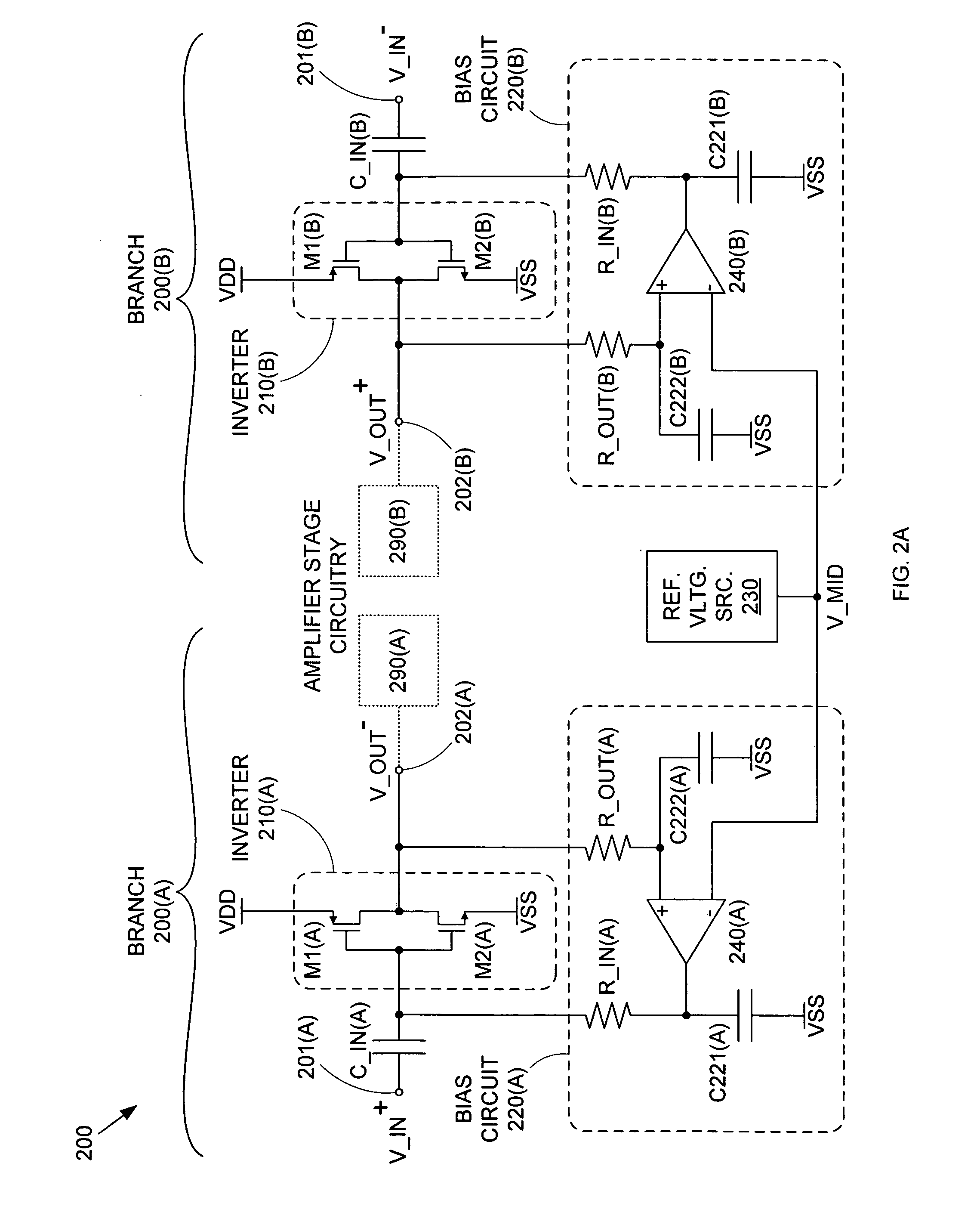
[0024]FIG. 2A shows a high-frequency amplifier circuit 200 in accordance with an embodiment of the invention. Amplifier circuit 200 is formed from two branches 200(A) and 200(B). Branch 200(A) includes an input terminal 201(A), an output terminal 202(A), a CMOS inverter 210(A), a capacitor C_IN(A), and a bias circuit 220(A). Capacitor C_IN(A) is coupled between input terminal 201(A) and the input of inverter 210(A) and provides DC filtering at the input of inverter 210(A). Bias circuit 220(A) is connected between the output and input of inverter 210(A).

[0025] Inverter 210(A) includes a PMOS transistor M1(A) and an NMOS transistor M2(A) that are serially coupled between an upper supply voltage VDD and a lower supply voltage (e.g., ground). The gate terminals of transistors M1(A) and M2(A) are connected to form the input of inverter 210(A), while the drain terminals of transistors M1(A) and M2(A) are connected to form the output of inverter 210(A).

[0026] Branch 200(B) is substantial...


PUM


Abstract

A differential CMOS amplifier includes two CMOS inverters and biasing circuitry providing feedback loops across the output and input of each inverter. The biasing circuitry provides linear biasing so that the inverters can apply a desired gain to a pair of high frequency input signals (i.e., a differential input signal). The biasing circuitry can include operational amplifiers (op-amps) for providing positive feedback control between the output and input of the inverters. The inputs of the inverters can be regulated by this feedback loop such that their outputs are driven to the reference voltage, thereby forcing the inverters to operate in their linear regions so that non-distorting amplification can be applied to the input AC signals.

Description

BACKGROUND [0001] 1. Field of the Invention [0002] The invention relates to the field of high frequency communications, an in particular to a complementary metal-oxide-semiconductor high frequency amplifier. [0003] 2. Related Art [0004] A differential amplifier is a fundamental electronic circuit that generates an output signal based on the difference between two input signals (a differential input signal). The output signal is therefore representative of the magnitude of the difference between the two input signals. To reduce costs (which is particularly important for consumer goods such as cellular telephones), differential amplifiers are often implemented using a metal-oxide-semiconductor (MOS) or complementary MOS (CMOS) process instead of the more expensive bipolar process. [0005]FIG. 1 shows a conventional RF MOS differential amplifier 100. MOS differential amplifier 100 includes input terminals 101-1 and 101-2, capacitors C1_IN, C2_IN, and C_GND, NMOS resistors R1_SET, R2_SET...

Claims


Application Information

Patent Timeline
Patent Type & Authority Applications(United States)
IPC IPC(8): G01R19/00H03F1/02H03F1/30H03F1/32
CPCH03F1/301H03F2200/54H03F2200/42H03F1/3205
Inventor MORAVEJI, FARHOOD
Owner SONRAI MEMORY LTD
Why Eureka
Try Eureka